Epitaxial wafer and switch element and light-emitting element using same

a switch element and epitaxial layer technology, applied in the field of epitaxial wafers, can solve the problems of not satisfying the requirements of electronic elements, the quality of the wafer, and the substrate including silicon carbide, so as to reduce the flux of the reaction source, minimize the defects of the epitaxial layer, and reduce the effect of internal defects

Active Publication Date: 2017-10-17
LX SEMICON CO LTD
View PDF13 Cites 1 Cited by
  • Summary
  • Abstract
  • Description
  • Claims
  • Application Information

AI Technical Summary

Benefits of technology

[0017]As described above, according to the embodiment, the internal defects and surface defects of the epitaxial layer can be minimized by reducing the flux of the reaction source to initially grow the epitaxial material at a low speed.
[0018]According to the embodiment, the internal defects and the surface defects of the epitaxial layer can be minimized by reducing the flux of Si to initially grow the epitaxial material at a low speed
[0019]According to the embodiment, the internal defects and the surface defects of the epitaxial layer can be minimized by reducing the flux of the growth source and the flux of the doping source to initially grow the epitaxial material at the low speed.
[0020]Accordingly, the epitaxial wafer having minimized internal defects and surface defects is applied to the electronic element, so that the characteristic required for the relevant electronic element can be satisfied.
[0021]According to the embodiment, even if the growth condition is changed, the growth is continued so that the semiconductor layer growth is not stopped between the first and third semiconductor layers. Therefore, defects can be more reduced, and the efficiency in the growth process can be enhanced, so that the process time can be reduced.

Problems solved by technology

Although conventional electronic elements are fabricated using sapphire or silicon, the sapphire or the silicon does not satisfy the requirements of the electronic elements.
However, the quality of wafers, which serves as a substrate including silicon carbide, is not satisfactory.

Method used


Image

  • Epitaxial wafer and switch element and light-emitting element using same
  • Epitaxial wafer and switch element and light-emitting element using same
  • Epitaxial wafer and switch element and light-emitting element using same

Examples


first embodiment

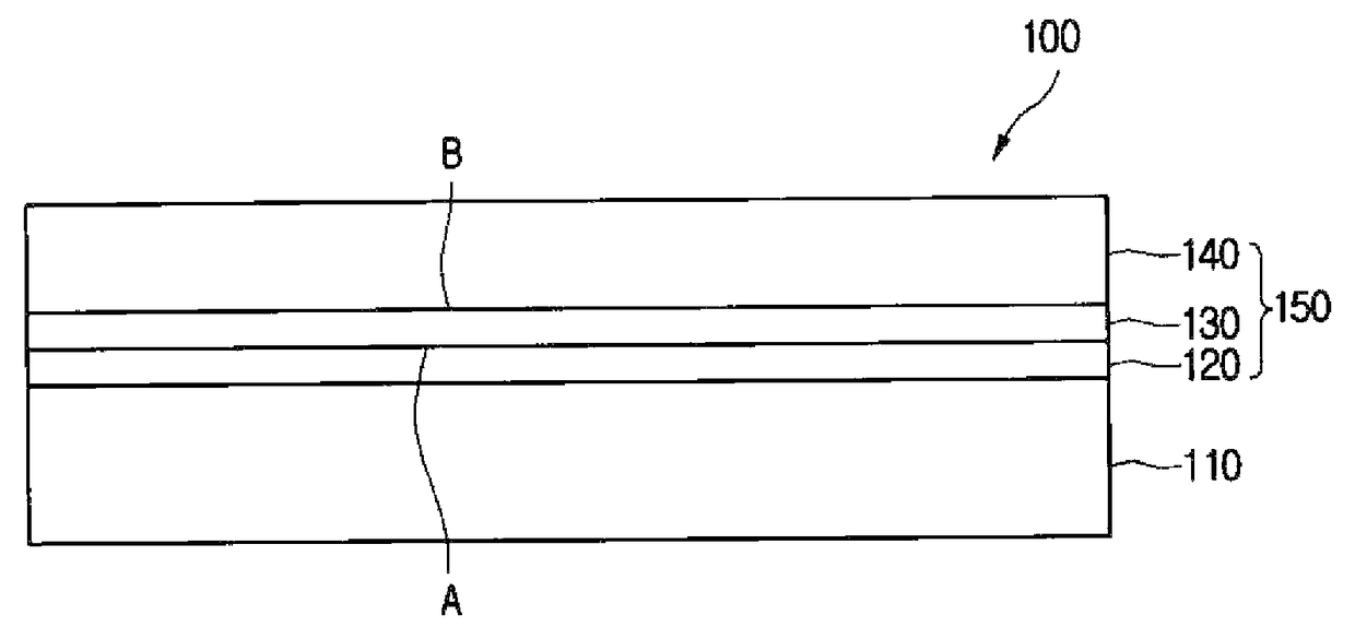
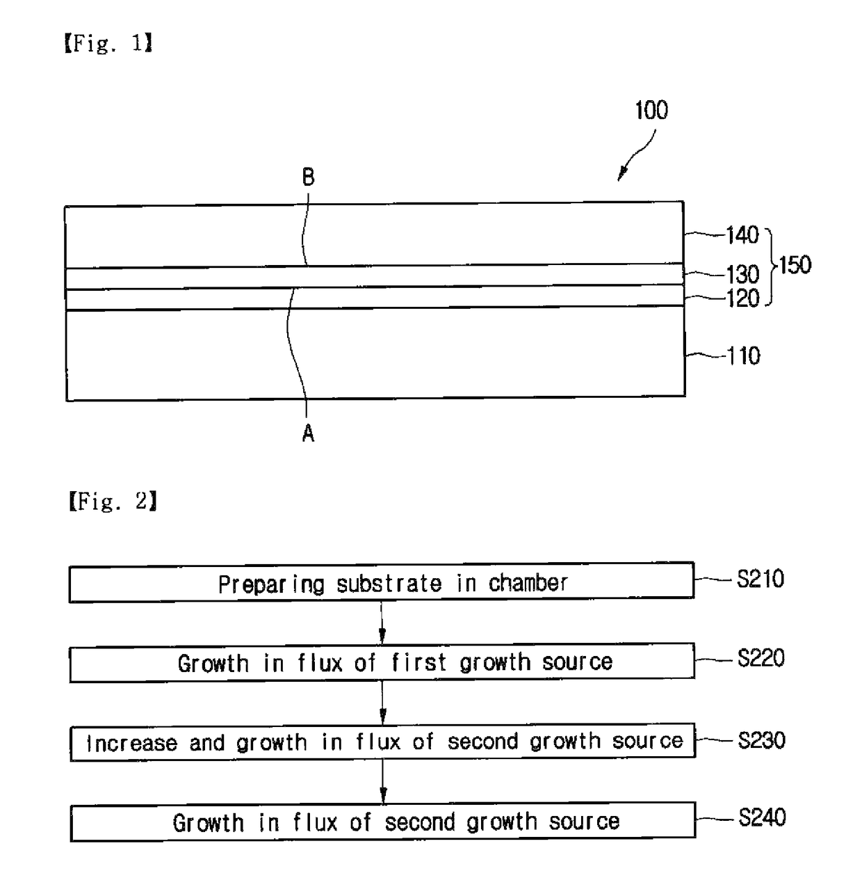
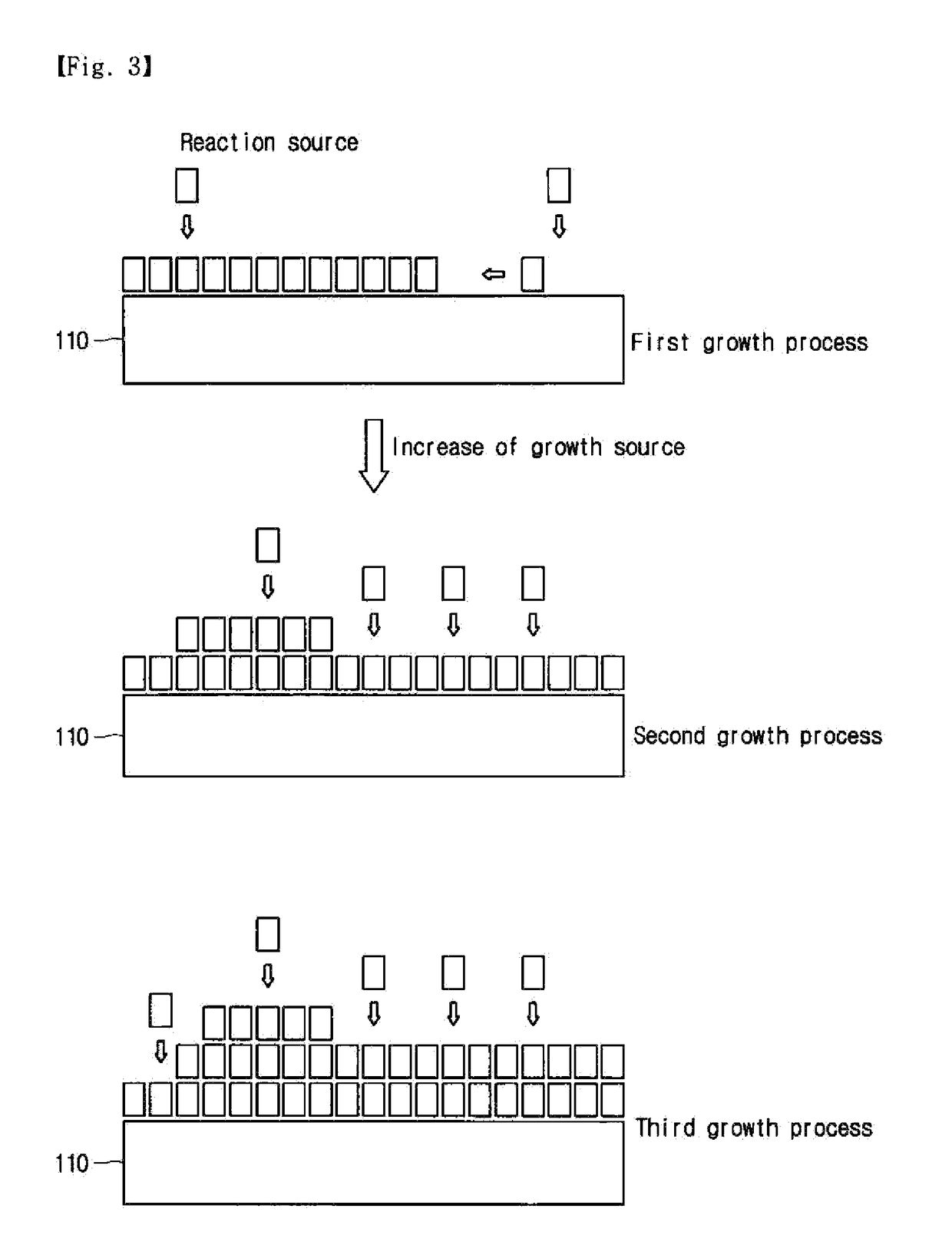
[0066]FIG. 2 is a flowchart showing the fabricating process of an epitaxial wafer of FIG. 1 according to a FIG. 3 shows the fabricating process of FIG. 2.

[0067]Referring to FIGS. 2 and 3, the substrate 110 may be provided in a reaction chamber (S210).

[0068]Although the substrate 110 may include one of 3C—SiC, 4H—SiC and 6H—SiC for the illustrative purpose, the material constituting the substrate 110 may be varied depending on an element or a product to be produced in the final stage.

[0069]The substrate 110 may be undoped or may be doped with an N type dopant or a P type dopant, but the embodiment is not limited thereto.

[0070]Before the substrate 110 is loaded into the reaction chamber, a cleaning process may be performed in order to remove an oxide layer naturally created on the surface of the substrate 110.

[0071]The substrate 110 may, for example have an off angle of about 0° to 10°, but the embodiment is not limited thereto. The off angle may be defined as an inclined angle of th...

second embodiment

[0112]FIG. 5 is a flowchart showing the fabricating process of the epitaxial wafer of FIG. 1 according to a

[0113]In the following description of the second embodiment, the structure or functions the same as those of the first embodiment have been described above, and the details thereof will be omitted. Those skilled in the art can easily understand the same structure of functions as those of the first embodiment by making reference to the description of the first embodiment.

[0114]Referring to FIG. 5, the substrate 110 may be provided in the reaction chamber (S310).

[0115]The substrate 110 may include one of 3C—SiC, 4H—SiC and 6H—SiC.

[0116]When the substrate 110 is provided, the reaction source may be introduced for the epitaxial growth in the reaction chamber.

[0117]The reaction source may include growth source for the epitaxial growth, doping source for doping, and dilution gas, but the embodiment is not limited thereto.

[0118]The epitaxial growth is performed on the substrate 110 th...


PUM


Abstract

An epitaxial wafer comprises an epitaxial layer disposed on a substrate. The epitaxial layer comprises first to third semiconductor layers. The third semiconductor layer has a thickness that is thicker than that of the first semiconductor layer. A second doping density of the second semiconductor layer is between a first doping density of the first semiconductor layer and a third doping density of the third semiconductor layer.

Description

TECHNICAL FIELD[0001]The embodiment relates to an epitaxial wafer.[0002]The embodiment relates to a method of fabricating an epitaxial wafer.[0003]The embodiment relates to a power element using an epitaxial wafer.[0004]The embodiment relates to a light-emitting element using an epitaxialBACKGROUND ART[0005]Electronic elements have been extensively used in the society at large.[0006]Although conventional electronic elements are fabricated using sapphire or silicon, the sapphire or the silicon does not satisfy the requirements of the electronic elements.[0007]Recently, researches and studies have been actively performed on electronic elements based on silicon carbide.[0008]However, the quality of wafers, which serves as a substrate including silicon carbide, is not satisfactory.DISCLOSURETechnical Problem[0009]The embodiment provides an epitaxial wafer having excellent quality.[0010]The embodiment provides an epitaxial wafer capable of minimizing defects.[0011]The embodiment provides...

Claims


Application Information

Patent Timeline
Patent Type & Authority Patents(United States)
IPC IPC(8): H01L29/16H01L29/34H01L29/24H01L21/02H01L33/34H01L33/26H01L33/22H01L33/00H01L29/872H01L29/36H01L33/02
CPCH01L29/1608H01L21/02378H01L21/02521H01L21/02529H01L29/24H01L29/34H01L29/36H01L29/872H01L33/0033H01L33/025H01L33/22H01L33/26H01L33/34H01L29/0878H01L29/7802
Inventor KANG, SEOK MINKIM, JI HYEHWANG, MIN YOUNG
Owner LX SEMICON CO LTD
Why Eureka
Try Eureka