Low noise InGaAs photodiode array

a photodiode array and low noise technology, applied in the field of low noise ingaas photodiode array, can solve the problems of physical isolation of the mesa device from the other, and the overall higher dark current, so as to minimize the read noise, reduce the dark current, and minimize the effect of dark curren

Active Publication Date: 2018-04-03
PRINCETON INFRARED TECH
View PDF29 Cites 0 Cited by
  • Summary
  • Abstract
  • Description
  • Claims
  • Application Information

AI Technical Summary

Benefits of technology

[0009]An array of photodiodes using InGaAs detectors for detecting visible and shortwave infrared light (e.g., wavelength range 0.5 to 2.7 μm) and has a buried p-n or p-i-n junction photodiode to reduce the dark current is disclosed. These detector arrays are hybridized to a Read Out Integrated Circuit (ROIC) or a multiplexer, which is an array of read out circuits that have amplification circuits and the ability to store charge from each detector in the detector array. The combination of detector, amplification and charge storage forms a pixel, and the combined unit of ROIC and detector array is called a focal plane array. In this design the photodiode is not directly connected to the ROIC amplification circuit typically manufactured in a complementary metal-oxide-semiconductor (CMOS) process. To allow the charge to be removed from the photodiode to the ROIC a junction field effect Transistor (JFET) is also integrated in every detector pixel. The drain of the JFET is connected to the ROIC while the source is the buried photodiode. Separating the photodiode from the amplification circuit minimizes read noise from the ROIC as well as dark current on the photodiode. The photodiode is truly at zero bias thus minimizing dark current. In addition burying the photodiode minimizes surface defects as well as defects caused by forming a contact to the diode.

Problems solved by technology

However, mesa devices are isolated from one another physically.
In a mesa device the physical isolation prevents cross talk between pixels and causes a loss in some signal and leads to overall higher dark current because the surfaces are not passivated.

Method used


Image

  • Low noise InGaAs photodiode array
  • Low noise InGaAs photodiode array
  • Low noise InGaAs photodiode array

Examples


Embodiment Construction

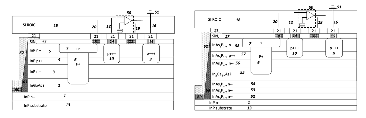
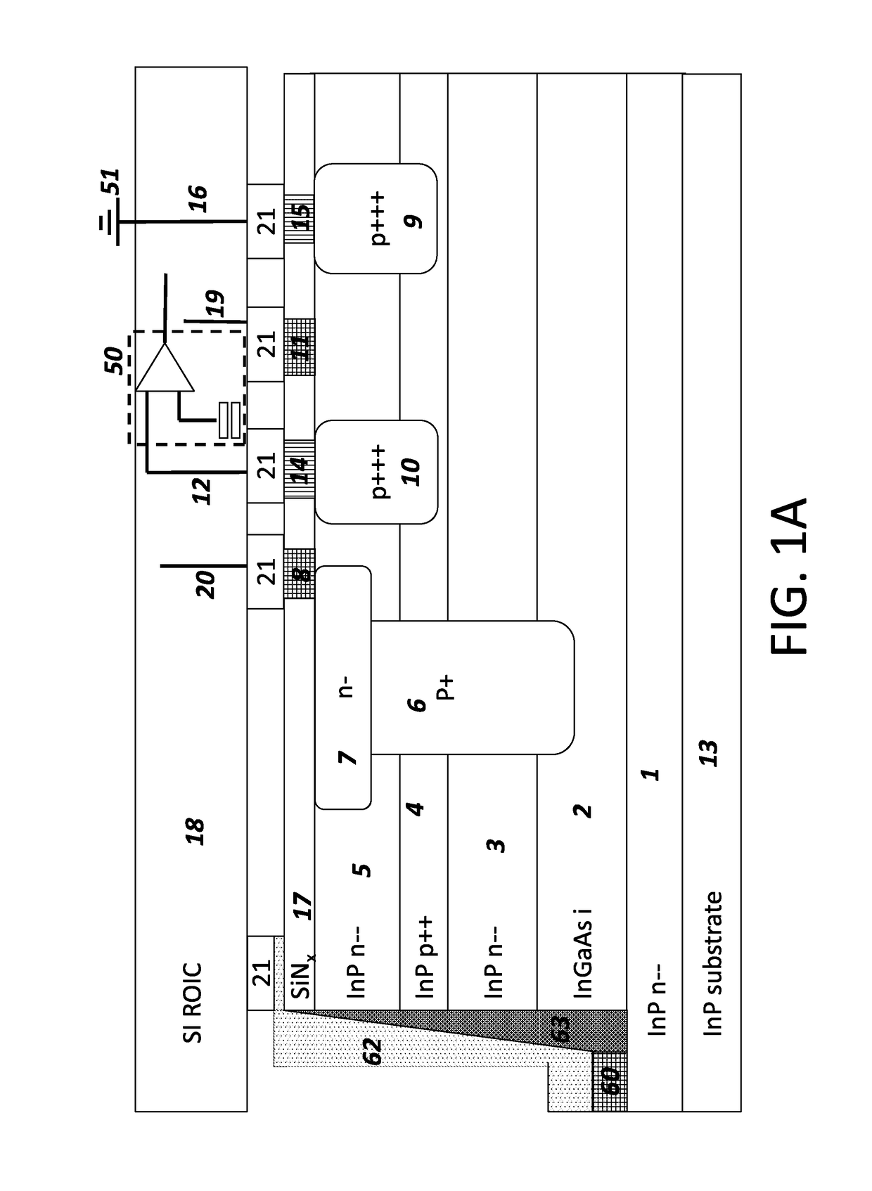
[0025]The present disclosure describes planar devices, which allow a complete interconnected array of pixels with no loss of material between pixels thus no loss in signal. In various implementations, an InGaAs detector array that has a buried photodiode (either p-n or p-i-n) and a junction field effect transistor (JFET) or multiple JFETs in each pixel to allow the movement of charge from the buried photodiode to a read out integrated circuit (ROIC) without the ROIC being directly connected to the photodiode. In some scenarios, the JFETs may be integrated to the photodetector in each pixel to allow movement of charge to the ROIC. A second JFET may be used to remove charge from the first JFET. This second JFET may be in each individual pixel or it may be a larger device that works an entire column or row simultaneously or 2 rows or 2 columns simultaneously. The multiple JFETs combined with the buried photodiode enables double correlated sampling in the pixel as well as lower capacita...


PUM


Abstract

A photodiode pixel structure for imaging short wave infrared (SWIR) and visible light built in a planar structure and may be used for one dimensional and two dimensional photodiode arrays. The photodiode arrays may be hybridized to a read out integrated circuit (ROIC), for example, a silicon complementary metal-oxide-semiconductor (CMOS) circuit. The photodiode in each pixel is buried under the surface and does not directly contact the ROIC amplification circuit. Charge is transferred form the detector using a junction field effect transistor (JFET) in each pixel. Disconnecting the photodiode from the ROIC amplification circuit enables low dark current as well as double correlated sampling in the pixel.

Description

CROSS REFERENCE TO RELATED APPLICATIONS[0001]The present application is a U.S. National Stage application of International Application No. PCT / US2014 / 057481, filed Sep. 25, 2014, which application claims the benefit of U.S. Provisional Application Ser. No. 61 / 882,385, filed on Sep. 25, 2013, the contents of each are hereby incorporated by reference in their entirety.FIELD OF THE DISCLOSURE[0002]This invention relates a device that allows for detection of visible and short wave infrared light with InxGa1-xAs detector arrays.BACKGROUND OF THE INVENTION[0003]Photodetector arrays made from indium gallium arsenide (InGaAs) alloys have been used in many applications, i.e. telecommunications, spectroscopy or imaging to name a few for over 25 years. Depending on the composition of the InxGa1-xAs alloy the detectors can detect light from 500 nm to 2700 nm. The most common composition is In0.53Ga0.47As, which is lattice matched to InP enabling detection from 0.5 um to 1.7 um. These can be man...

Claims


Application Information

Patent Timeline
Patent Type & Authority Patents(United States)
IPC IPC(8): H01L29/80H01L27/146H01L29/66H01L29/808H01L31/0304H01L31/105H01L31/18
CPCH01L27/14679H01L27/1461H01L27/1465H01L27/14609H01L27/14652H01L31/1844H01L29/66901H01L29/808H01L31/03046H01L31/105H01L27/14694H01L27/14612
Inventor ETTENBERG, MARTIN H.
Owner PRINCETON INFRARED TECH
Why Eureka
Try Eureka