
Semiconductor memory device and weak cell detection method thereof

Active Publication Date: 2017-11-21
SK HYNIX INC
View PDF11 Cites 1 Cited by
  • Summary
  • Abstract
  • Description
  • Claims
  • Application Information

AI Technical Summary

Benefits of technology

This patent is about a semiconductor memory device that can detect weak cells quickly through a test operation. The device includes a plurality of memory blocks, bit-line sense amplifiers shared by neighboring memory blocks, and a word line driver. The device can also have a weak cell detection circuit that compresses the amplified data to detect any weak cells. The technical effect of this invention is to provide a fast and efficient way to detect and fix problematic memory cells in a semiconductor memory device.

Problems solved by technology

Hence, the data stored in the capacitor may be lost without supplementing the stored charges.
Meanwhile, when the individual data retention times of weak memory cells included in a memory device is less than the reference retention time of the device, data errors may occur in the weak cells of the memory device, and thus, the memory device including the weak memory cells should be detected and abandoned.
Without an accurate test for detecting the weak memory cells in a semiconductor memory device, the reliability of the semiconductor memory device is damaged.
Also, generally, reliability problems due to weak memory cells may worsen as memory cell density increases.

Method used


Image

  • Semiconductor memory device and weak cell detection method thereof
  • Semiconductor memory device and weak cell detection method thereof
  • Semiconductor memory device and weak cell detection method thereof

Examples


first embodiment

[0058]FIG. 6 is a circuit diagram illustrating a weak cell detection circuit 100A in accordance with the present invention.

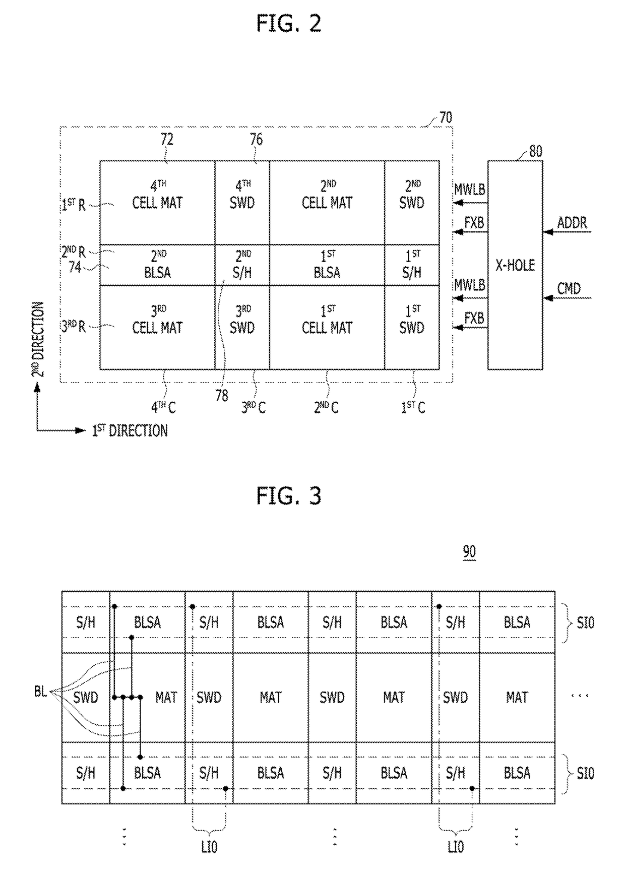
[0059]The weak cell detection circuit 100A in accordance with the first embodiment of the present invention may include a plurality of weak cell detectors 110A that respectively correspond to the plurality of bit-line sense amplifiers BLSA1 to BLSA8. Each of the weak cell detectors 110A may detect weak cells by compressing the data transferred through the corresponding upper and lower segment input / output line pairs SIO0:3> and SIOB0:3> and SIO4:7> and SIOB4:7> and mapping and outputting the compressed data to one among local input / output lines LIO0:7>.

[0060]FIG. 6 shows the weak cell detector 110A that detects weak cells by compressing the data that is sensed and amplified by corresponding one (e.g., the first bit-line sense amplifier BLSA1) of the odd-numbered bit-line sense amplifiers BLSA1, BLSA3, BLSA5 and BLSA7 and transferred through the upper segment inp...

second embodiment

[0071]FIG. 8 is a circuit diagram illustrating a weak cell detection circuit 300, in accordance with the present invention.

[0072]Referring to FIG. 8, the weak cell detection circuit 300 may include a plurality of data compression units 310 to 380 that correspond to a plurality of bit-line sense amplifiers BLSA1 to BLSA8, respectively. The plurality of data compression units 310 to 380 may be serially coupled to each other, and the last one of the plurality of data compression units 310 to 380 (e.g., the eighth data compression unit 380) may output corresponding compressed data SIO_SUM7> to the last lower local input / output line pair LIO7> and LIOB7> as a final test result TEST_OUT.

[0073]The respective data compression units 310 to 380 may receive data provided from the corresponding upper and lower segment input / output line pairs SIO0:3> and SIOB0:3> and SIO4:7> and SIOB4:7>. Further, the respective data compression units 310 to 380 may receive compressed data provided from the seri...

third embodiment

[0076]FIG. 9 is a circuit diagram illustrating a weak cell detection circuit 400, in accordance with the present invention.

[0077]Referring to FIG. 9, the weak cell detection circuit 400 may include a plurality of data compression units 410 to 480 that correspond to a plurality of bit-line sense amplifiers BLSA1 to BLSA8, respectively. The plurality of data compression units 410 to 480 may be serially coupled to each other, and the last one of the plurality of data compression units 410 to 480 (e.g., the eighth data compression unit 480) may output corresponding compressed data SIO_SUM7> to the last lower local input / output line pair LIO7> and LIOB7> as a final test result TEST_OUT.

[0078]The second to eighth data compression units 420 to 480 may compress a data transferred through a corresponding line among upper segment input / output lines SIO0:3> or lower segment input / output lines SIO4:7> with a compressed data outputted from the data compression unit of the previous stage together...


PUM


Abstract

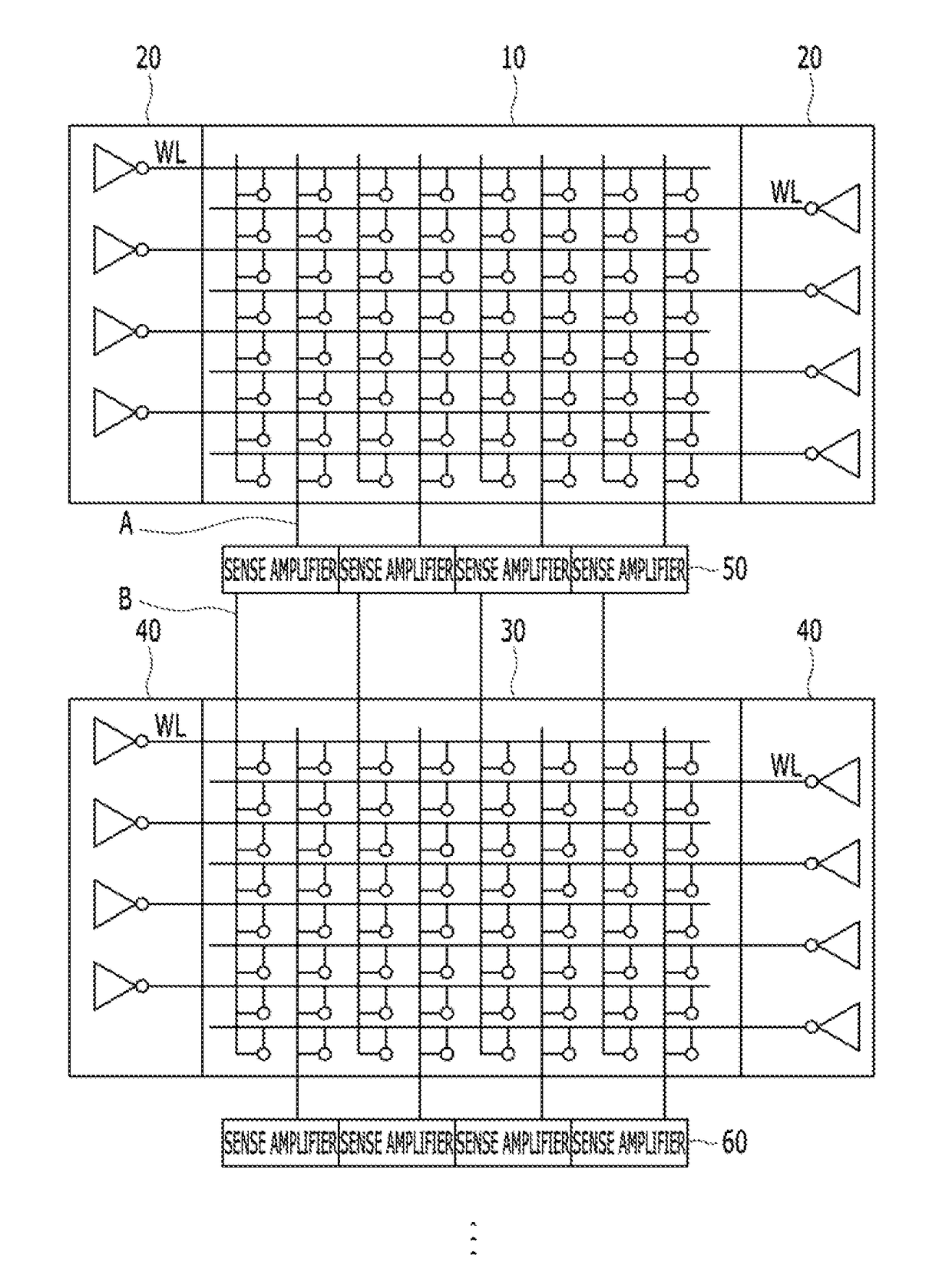
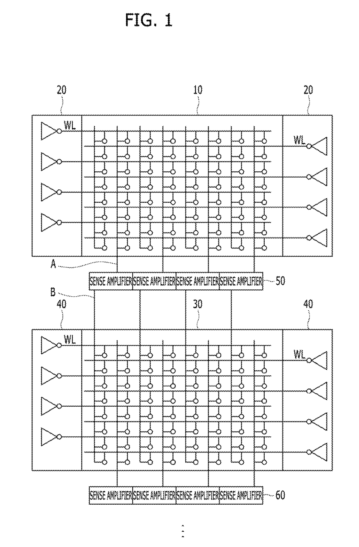
A semiconductor memory device includes: a plurality of memory blocks; a plurality of bit-line sense amplifiers shared by neighboring memory blocks among the plurality of the memory blocks, and suitable for sensing and amplifying data read from memory cells coupled to activated word lines through bit lines, and outputting the amplified data through a plurality of segment data lines; a word line driver suitable for activating word lines of memory blocks that do not share the bit-line sense amplifiers during a test mode; and a weak cell detection circuit suitable for compressing the amplified data transferred through the plurality of the segment data lines for generating compressed data and detecting a weak cell based on the compressed data during the test mode.

Description

CROSS-REFERENCE TO RELATED APPLICATIONS[0001]The present application claims priority of Korean Patent Application No. 10-2016-0060016, filed on May 17, 2016, which is Incorporated herein by reference in its entirety.BACKGROUND1. Field[0002]Exemplary embodiments of the present invention relate generally to a semiconductor designing technology, and more particularly, to a method for detecting a weak cell in a semiconductor memory device.2. Description of the Related Art[0003]Each memory cell of a semiconductor memory device, such as a dynamic random access memory (DRAM) device, generally includes a capacitor for storing data in the form of charges and a transistor functioning as a switch for controlling the flow of charges to and from the capacitor. Whether a data is in a ‘high logic’ level (i.e., logic ‘1’) or a ‘low logic’ level (i.e., logic ‘0’) is decided based on whether the capacitor stores the charges or not, in other words, whether the terminal voltage of the capacitor is high...

Claims


Application Information

Patent Timeline
IPC IPC(8): G11C7/00G11C11/4091G11C11/406G11C11/408G11C29/40G11C11/4093G11C29/00
CPCG11C29/40G11C11/4091G11C11/406G11C11/4085G11C11/4093G11C5/025G11C7/02G11C11/4097G11C2211/4068G11C29/50016G11C29/783
Inventor KIM, YOUK-HEE
Owner SK HYNIX INC
Learn More