Method for correcting wafer bow from overlay

a technology of wafers and bows, applied in the field of wafer overlays, can solve the problems of overlay errors, expansion exceeds overlay error requirements, and large overlay errors, and achieve the effect of improving the overlay

Active Publication Date: 2017-11-21
TOKYO ELECTRON LTD
View PDF14 Cites 3 Cited by
  • Summary
  • Abstract
  • Description
  • Claims
  • Application Information

AI Technical Summary

Benefits of technology

[0007]Other fabrication steps can also cause substrate expansion and contraction. For example, deposited films can cause substrate contraction. Also, various annealing and doping steps can create substantial amounts of bow in a given substrate. Annealing steps can especially create overlay challenges. The result of these various fabrication steps is a substrate that is uneven or non-planar. For example, a backside of the substrate can have z-height differences (differences in vertical heights) that have both high spots and low spots. Such height differences due to such bowing can be on the order of about a micron to approximately 100 microns. This fluctuation is significant because semiconductor devices or structures being exposed by various exposure tools are being exposed on scales of tens of nanometers to hundreds of nanometers. Thus having deflection variations of thousands of nanometers to 10,000 nanometers can dramatically reduce yield.
[0009]Techniques disclosed herein include methods for flattening a substrate, which flattening can improve overlay. In an example method, a substrate is received for processing. This substrate has multiple semiconductor structures that are at least partially fabricated on a top surface of the substrate. The substrate has a backside surface that is non-planar. The backside surface being non-planar as a result of fabrication of the multiple semiconductor structures. The backside surface is opposite the top surface. Deflection areas are identified on the backside surface of the substrate. Particles are directed to strike the backside surface of the substrate based on identified deflection areas on the backside surface of the substrate, thereby causing the backside surface to become planar, which enables subsequent microfabrication steps to be successful.

Problems solved by technology

Any movement of the substrate relative to the substrate stage after alignment, however, can result in overlay errors.
If the substrate expansion is unchecked, the expansion exceeds overlay error requirements.
Moreover, if the clamping force between the substrate and the substrate chuck is not sufficient to prevent substrate expansion, then the substrate can slip on the substrate chuck and larger substrate expansion will occur, resulting in larger overlay errors.
Thus, vacuum clamping is not always possible, and the weaker electrostatic clamping must be used in lieu of a vacuum clamp.
Other fabrication steps can also cause substrate expansion and contraction.
For example, deposited films can cause substrate contraction.
Also, various annealing and doping steps can create substantial amounts of bow in a given substrate.
Annealing steps can especially create overlay challenges.
The result of these various fabrication steps is a substrate that is uneven or non-planar.
With such significant bowing, however, it can be very difficult or impossible to accurately flatten a substrate by chucking a substrate alone.

Method used


Image

  • Method for correcting wafer bow from overlay
  • Method for correcting wafer bow from overlay
  • Method for correcting wafer bow from overlay

Examples


Embodiment Construction

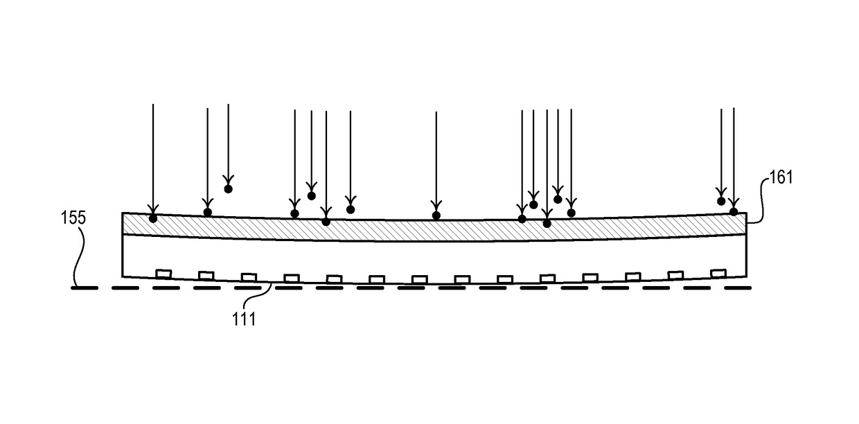
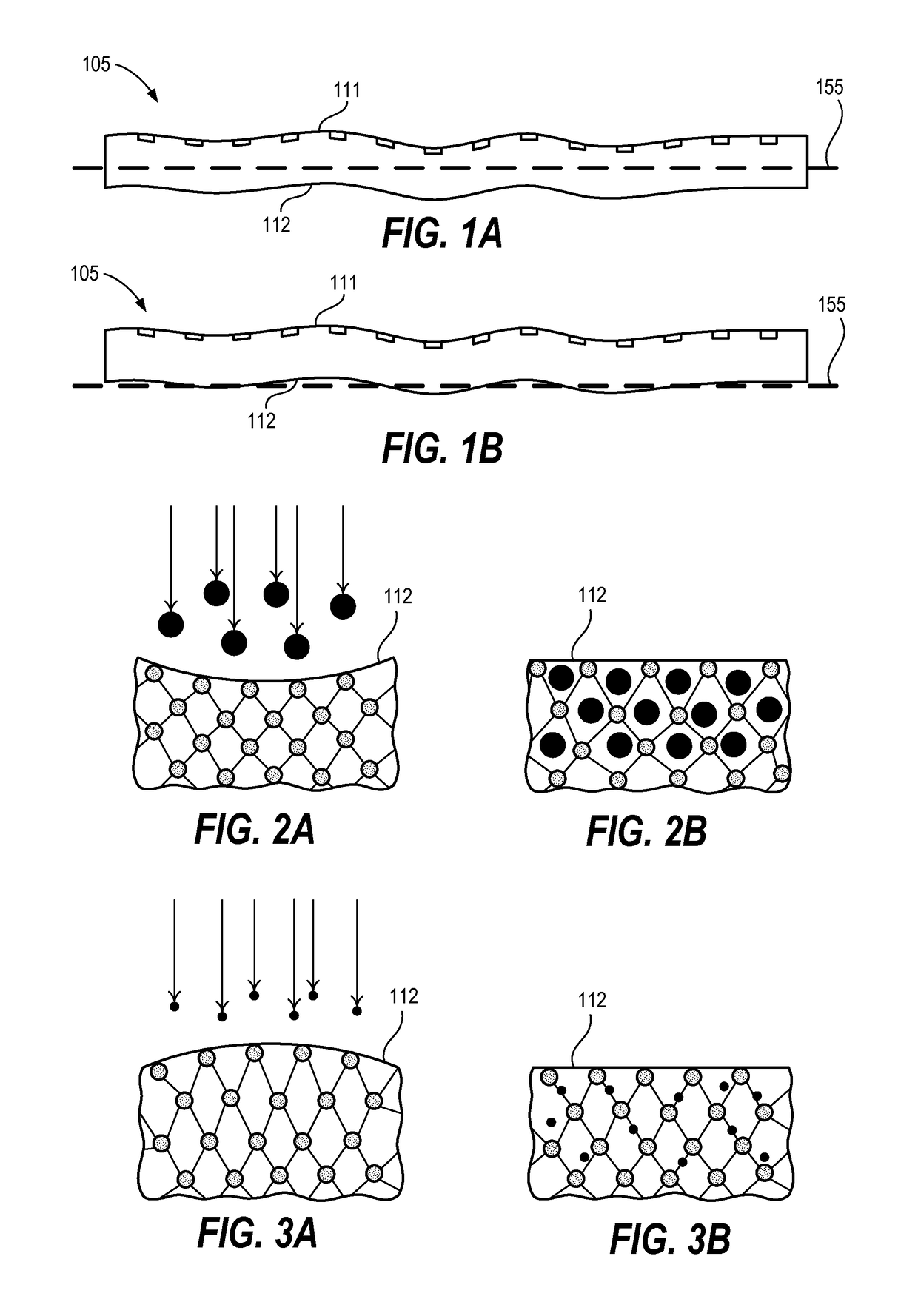
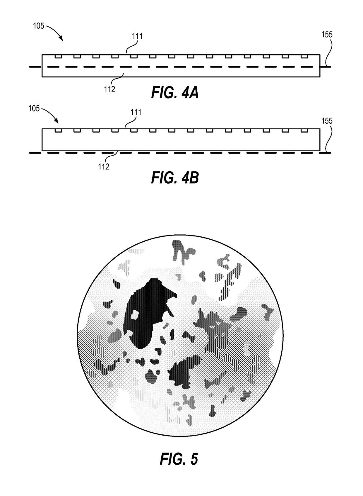
[0028]Techniques include treating a backside or backside surface of a substrate with particles of varying doses, densities, and spatial locations such that stress controlled by inside energies due to the substrate interaction changes the substrate bow to improve overlay. In other words, techniques herein included targeted particle bombardment of a substrate backside surface to flatten a substrate or cause the substrate to become more planar by reducing points of deflection. The top side of a substrate (opposite that of backside) typically receives a film stack, fabricated devices, partially fabricated devices, features, etc. Thus, the top side of the substrate can also be known as a working surface. In semiconductor fabrication, substrates typically become warped or bowed due to the overlay of various films and devices being deposited and / or fabricated thereon. Such processes can include annealing and other treatments that tend to warp a substrate. Techniques herein, however, correc...


PUM

PropertyMeasurementUnit
heightaaaaaaaaaa
height deviationaaaaaaaaaa
heightaaaaaaaaaa

Abstract

Described herein are methods for flattening a substrate, such as a semiconductor wafer, to reduce bowing in such substrates. Methods include treating or bombarding a backside surface of a substrate with particles of varying doses, densities, and spatial locations. Particle bombardment and selection is such that the substrate becomes more planar by selectively increasing or decreasing z-height points to reduce overall deflection. One or more tensile or compressive films can be added to the backside surface to be selectively relaxed at specific point locations. Such methods can correct bowing in substrates resulting from various fabrication processes such as thermal annealing.

Description

CROSS REFERENCE TO RELATED APPLICATIONS[0001]The present application claims the benefit of U.S. Provisional Patent Application No. 61 / 977,282, filed on Apr. 9, 2014, entitled “Method for Correcting Wafer Bow from Overlay,” which is incorporated herein by reference in its entirety.BACKGROUND OF THE INVENTION[0002]This disclosure relates to semiconductor fabrication, and particularly to wafer overlay.[0003]Semiconductor fabrication involves multiple varied steps and processes. One typical process is known as photolithography (also called microlithography). Photolithography uses radiation, such as ultraviolet or visible light, to generate fine patterns in a semiconductor device design. Many types of semiconductor devices, such as diodes, transistors, and integrated circuits, can be fabricated using semiconductor fabrication techniques including photolithography, etching, film deposition, surface cleaning, metallization, and so forth.[0004]Exposure systems (also called tools) are used t...

Claims


Application Information

Patent Timeline
Patent Type & Authority Patents(United States)
IPC IPC(8): H01L21/265H01L21/30H01L21/66H01L21/302
CPCH01L21/2658H01L21/265H01L22/20H01L21/302H01L22/12
Inventor DEVILLIERS, ANTON J.
Owner TOKYO ELECTRON LTD
Why Eureka
Try Eureka