Method for manufacturing monocrystalline graphene
a monocrystalline graphene and graphene technology, applied in the direction of polycrystalline material growth, crystal growth process, chemically reactive gas, etc., can solve the problem that the thickness of high-integrated semiconductor devices equal to or less than 30 nm cannot be easily manufactured, the electrodes cannot be easily patterned using electron beam lithography,
- Summary
- Abstract
- Description
- Claims
- Application Information
AI Technical Summary
Benefits of technology
Problems solved by technology
Method used
Image

Examples
Embodiment Construction
Technical Problem
[0010]The present invention provides a method of growing a graphene layer oriented in a direction, e.g., a monocrystalline graphene layer, on a wafer-scale insulating substrate. However, the scope of the present invention is not limited thereto.
Technical Solution
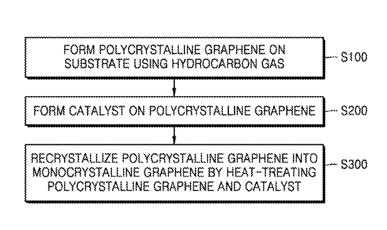
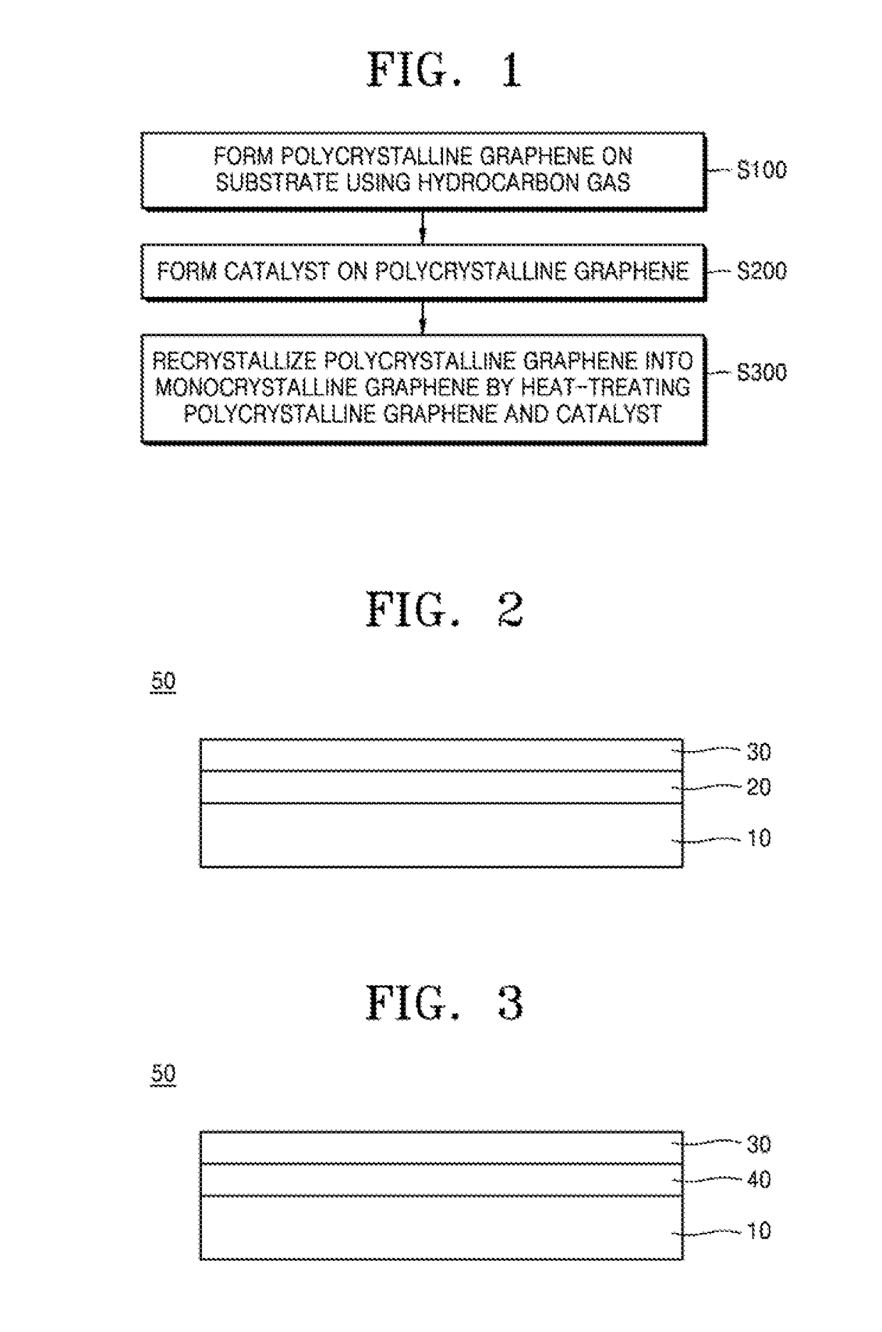
[0011]According to an aspect of the present invention, there is provided a method of manufacturing monocrystalline graphene, the method including forming polycrystalline graphene on a substrate using a hydrocarbon gas, forming a catalyst on the polycrystalline graphene, and recrystallizing the polycrystalline graphene into monocrystalline graphene by heat-treating the polycrystalline graphene and the catalyst.
[0012]The substrate may be an insulating substrate including Al2O3, AlN, Si3N4, SrTiO3, or BN. Alternatively, the substrate may be a composite substrate obtained by growing a transition metal including copper (Cu) or nickel (Ni) in a form of a thin layer having a thickness of 0.5 μm to 3 μm, on the insu...
PUM
| Property | Measurement | Unit |
|---|---|---|
| thickness | aaaaa | aaaaa |
| temperature | aaaaa | aaaaa |
| temperature | aaaaa | aaaaa |
Abstract
Description
Claims
Application Information
 - R&D
- Intellectual Property
- Life Sciences
- Materials
- Tech Scout
- Unparalleled Data Quality
- Higher Quality Content
- 60% Fewer Hallucinations
Browse by: Latest US Patents, China's latest patents, Technical Efficacy Thesaurus, Application Domain, Technology Topic, Popular Technical Reports.
© 2025 PatSnap. All rights reserved.Legal|Privacy policy|Modern Slavery Act Transparency Statement|Sitemap|About US| Contact US: help@patsnap.com