Printed wiring board, electronic device, and wiring connection method

a technology of electronic devices and printed wiring boards, applied in the direction of printed element electric connection formation, high frequency circuit adaptation, waveguides, etc., can solve the problems of parasitic stubs, wiring boards that penetrate the printed wiring boards completely, and discontinuity of impedance in transmission lines, etc., to achieve low cost, alleviate parasitic stub discontinuity in transmission lines, and improve the effect of transmission line stability

Inactive Publication Date: 2018-01-02
NEC CORP
View PDF16 Cites 1 Cited by
  • Summary
  • Abstract
  • Description
  • Claims
  • Application Information

AI Technical Summary

Benefits of technology

[0027]According to an exemplary embodiment of the present invention, impedance discontinuity in a transmission line caused by a parasitic stub can be alleviated. For this reason, the printed wiring board enabling higher-speed data communication can be provided with low cost.

Problems solved by technology

As a result, the tendency that a loss of a signal, a noise, and a cross talk between wirings occur becomes high.
However, a through-hole formed in the above-described printed wiring board penetrates the printed wiring board entirely.
It is known that this parasitic stub produces discontinuity of impedance in the transmission line, and becomes a factor of a signal loss and the like.
It is known that in the case of 10 Gbase-KR, a loss caused by a stub parasitic on a through-hole for mounting a backplane connector is particularly large.
This leads to a cause for impedance mismatch that is not intended by a designer, and causes degradation in quality of high-frequency signal propagating through the transmission line.

Method used


Image

  • Printed wiring board, electronic device, and wiring connection method
  • Printed wiring board, electronic device, and wiring connection method
  • Printed wiring board, electronic device, and wiring connection method

Examples


Embodiment Construction

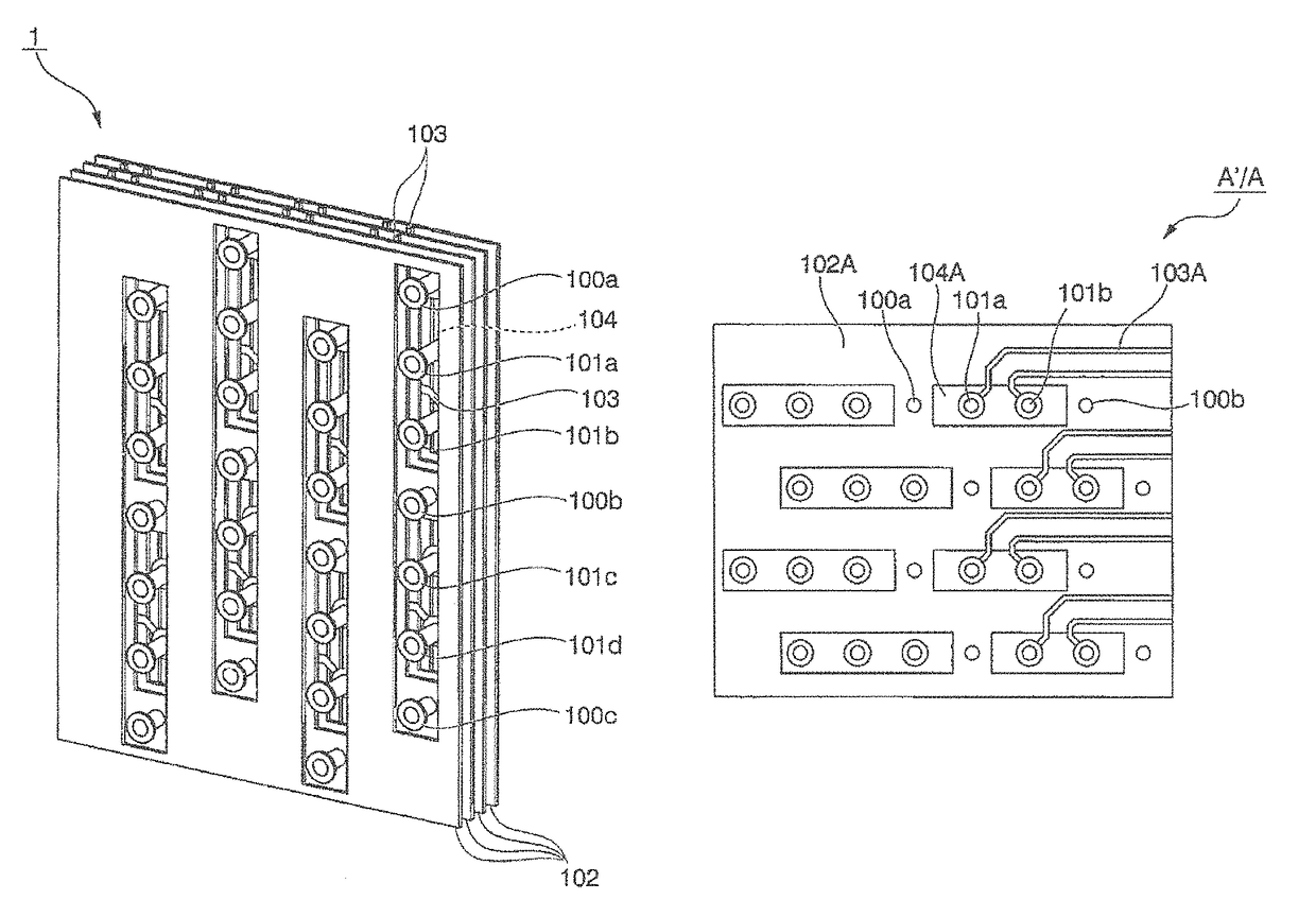
[0039]In the following, a printed wiring board according to an exemplary embodiment of the present invention is explained with reference to drawings.

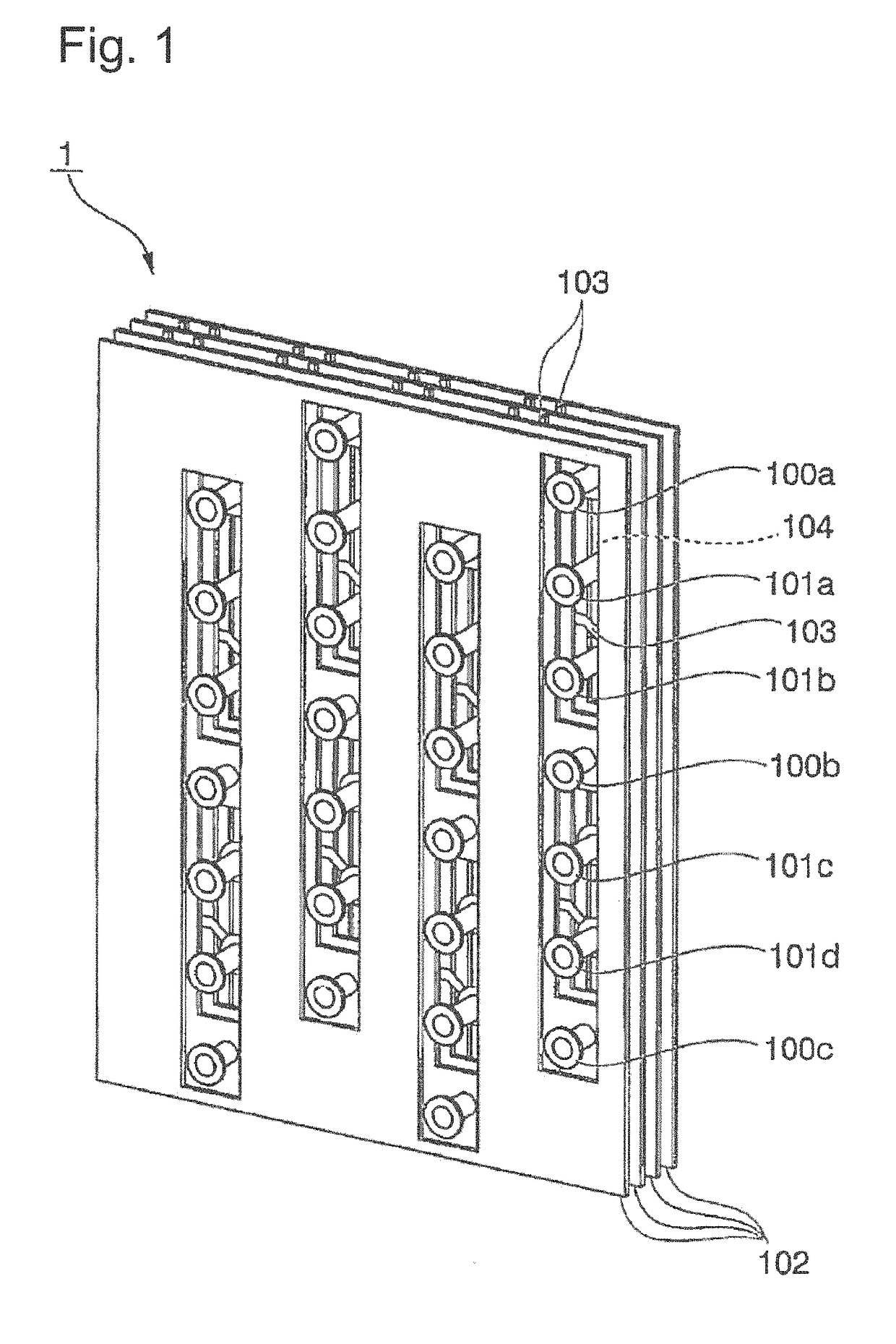
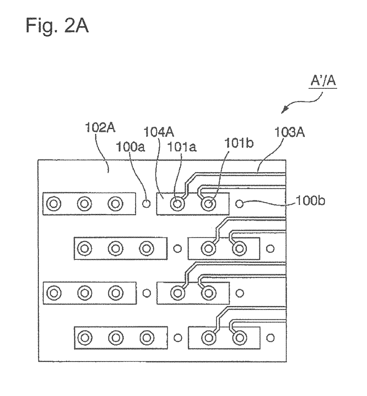
[0040]FIG. 1 is a first diagram illustrating a configuration of the printed wiring board according to an exemplary embodiment of the present invention.

[0041]As illustrated in FIG. 1, the printed wiring board 1 is configured by stacking a large number of ground layers and wiring layers via insulating layers. The ground layers and the wiring layers are each a conductor layer. Although insulating layers are omitted in FIG. 1 for convenience of explanation, the insulating layer actually exists between the respective conductor layers (refer to FIG. 3). The insulating layer is formed by a dielectric substance such as a resin.

[0042]The ground layer includes a ground plane 102 formed as a conductor pattern. This ground plane 102 functions as a ground. The wiring layer includes a signal wiring 103 formed as a conductor pattern. By the conductor ...


PUM

PropertyMeasurementUnit
frequencyaaaaaaaaaa
frequencyaaaaaaaaaa
frequencyaaaaaaaaaa

Abstract

A printed wiring board is provided with a wiring layer, a first ground layer, a second ground layer, a grounding through-hole, a signal through-hole, a first clearance, and a second clearance. The wiring layer has a signal line. The first ground layer has a first ground plane. The second ground layer is positioned between the wiring layer and the first ground layer and has a second ground plane. The grounding through-hole passes through the wiring layer, the first ground layer, and the second ground layer and is connected to the second ground plane. The signal through-hole passes through the wiring layer, the first ground layer, and the second ground layer and is connected to the signal line. The first clearance is formed in the first ground layer, is positioned in the vicinity of the signal through-hole and the grounding through-hole, and separates the first ground plane from the signal through-hole and the grounding through-hole. The second clearance is formed in the second ground layer, is positioned in the vicinity of the signal through-hole, and separates the second ground plane from the signal through-hole.

Description

TECHNICAL FIELD[0001]The present invention relates to a printed wiring board mainly used in transmission of high-frequency differential signals, an electronic device, and a wiring connection method.BACKGROUND ART[0002]Many of recent electronic devices improve an integration degree in a circuit by using a printed wiring board in which a plurality of insulating layers and a plurality of conductive layers (wiring layers) are stacked. In this case, a wiring formed in each wiring layer is usually connected to a hole penetrating all layers in the board, by a conductor (referred to as a “through-hole” in the following) with which the inner surface of the hole is plated.[0003]In the field of data communication such as Ethernet (Registered Trademark), a data forwarding speed becomes higher year by year. Recently, particularly, to increase a speed of transmitting an electric signal, differential signals, e.g., have been used. This is an idea for reducing influence of a noise from an outside, ...

Claims


Application Information

Patent Timeline
Patent Type & Authority Patents(United States)
IPC IPC(8): H01P3/08H01P3/02H05K1/11H05K3/42H05K1/02
CPCH01P3/082H01P3/026H05K1/0224H05K1/0251H05K1/116H05K3/429H05K1/0253Y10T29/49167H05K1/0245H05K2201/09718
Inventor KASHIWAKURA, KAZUHIRO
Owner NEC CORP
Why Eureka
Try Eureka