Vibrating device

a technology of vibration device and tcf, which is applied in the direction of piezoelectric/electrostrictive/magnetostrictive devices, electrical apparatus, impedence networks, etc., can solve the problem of difficulty in sufficiently reducing the absolute value of tcf, and achieve the effect of satisfying temperature characteristics

Active Publication Date: 2018-01-09
MURATA MFG CO LTD
View PDF60 Cites 1 Cited by
  • Summary
  • Abstract
  • Description
  • Claims
  • Application Information

AI Technical Summary

Benefits of technology

[0010]An object of the present invention is to provide a vibrating device capable of further reducing an absolute value of the temperature coefficient of resonant frequency (TCF).

Problems solved by technology

However, those disclosed methods have a difficulty in sufficiently reducing the absolute value of the TCF.

Method used


Image

  • Vibrating device
  • Vibrating device
  • Vibrating device

Examples


first embodiment

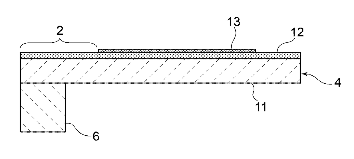
[0073]FIG. 10(a) is a front sectional view of a vibrating device according to a modification of the present invention. FIG. 10(b) is a front sectional view, partly cut-away, of an excitation portion used in the vibrating device according to the modification.

[0074]In the vibrating device according to the modification of the first embodiment, as illustrated in FIG. 10(a), the silicon oxide layer 12 is laminated on one principal surface of the Si layer 11. An excitation portion 17 is laminated on the other principal surface of the Si layer 11. The excitation portion 17 includes the piezoelectric thin film 14 and the first electrode 15. In this modification, the second electrode 16 is not separately provided, and the Si layer 11 serves also as the second electrode. Additionally, the first electrode 15 is not buried in the piezoelectric thin film 14.

[0075]The piezoelectric thin film 14 and the first electrode 15 are laminated on the Si layer 11 in the mentioned order. Because of the Si l...

second embodiment

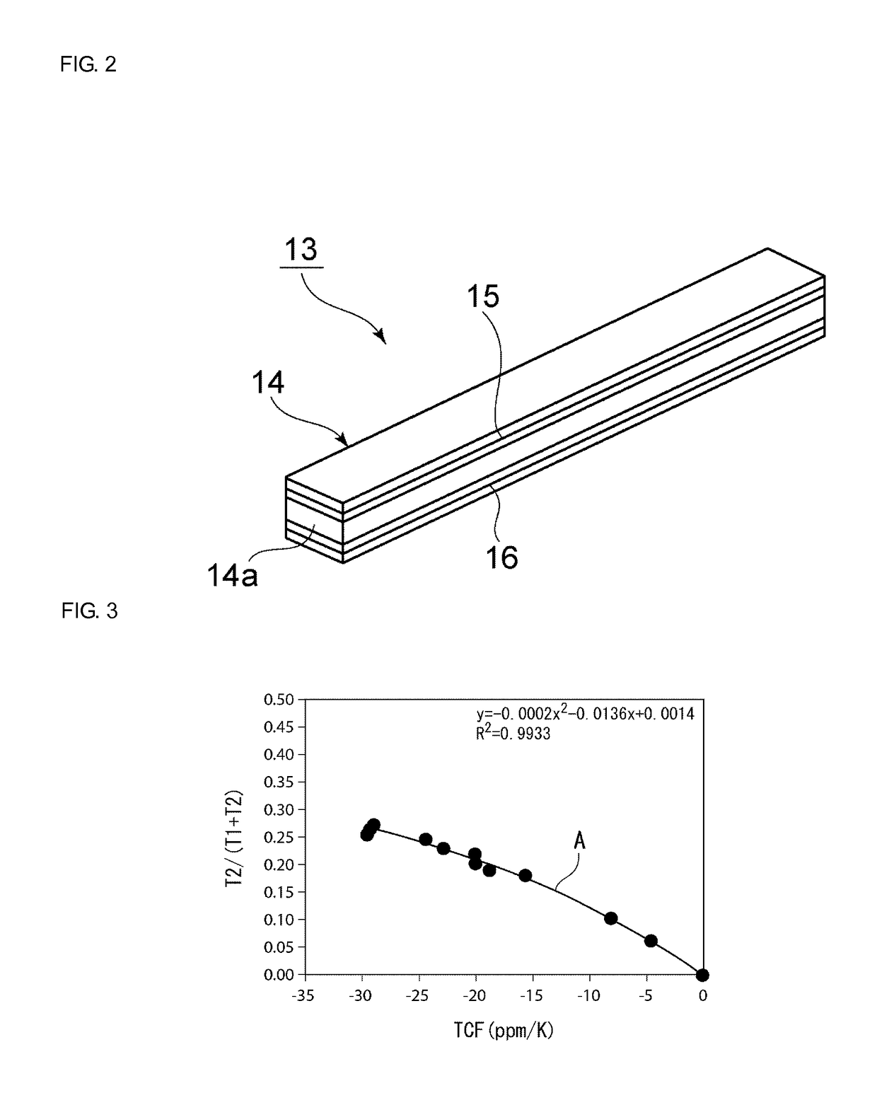
[0081]Also in the second embodiment, it is just required that, assuming the thickness of the Si layer 11 in each of the tuning fork arms 23 to 26 is denoted by T1 and the total thickness of the silicon oxide layers 12a and the silicon oxide layer 12b is denoted by T2, the thickness ratio T2 / (T1+T2) is within the range expressed by the above-described formula (1). Under such a condition, the absolute value of the temperature coefficient of resonant frequency (TCF) can be kept within ±5 ppm / ° C.

[0082]Furthermore, according to the second embodiment, since the silicon oxide layers 12a and 12b are provided at both the sides of the Si layer 11, warping of the Si layer 11 can be suppressed.

[0083]In addition, according to the second embodiment, since the number of the tuning fork arms vibrating in one phase is equal to the number of the tuning fork arms vibrating in the opposite phase, vibration characteristics can be improved from those in the first embodiment.

[0084]Stated in another way, ...


PUM


Abstract

A vibrating device having tuning fork arms extending in a first direction that are joined to a base portion and are arranged side by side in an second direction. Each of the tuning fork arms has a structure that a silicon oxide layer is laminated on a Si layer made of a degenerate semiconductor, and that an excitation portion is provided on the silicon oxide layer. When a total thickness of the Si layer is denoted by T1, a total thickness of the silicon oxide layer is denoted by T2, and the temperature coefficient of resonant frequency (TCF) when the silicon oxide layer is not provided on the Si layer is denoted by x, a thickness ratio T2 / (T1+T2) is within a range of (−0.0002x2−0.0136x+0.0014)±0.05.

Description

CROSS REFERENCE TO RELATED APPLICATIONS[0001]The present application is a continuation of International application No. PCT / JP2014 / 062079, filed May 1, 2014, which claims priority to Japanese Patent Application No. 2013-101300, filed May 13, 2013, the entire contents of each of which are incorporated herein by reference.FIELD OF THE INVENTION[0002]The present invention relates to a vibrating device including a plurality of tuning fork arms, and more particularly to an MEMS vibrating device.BACKGROUND OF THE INVENTION[0003]An MEMS (Micro Electro Mechanical Systems) structure is so far known in which an excitation portion including a piezoelectric thin film is constituted on a Si semiconductor layer. Various trials have been made to improve the temperature coefficient of resonant frequency (TCF) in a vibrator with the MEMS structure. Patent Document 1, given below, discloses a method of reducing an absolute value of the TCF by laminating Si and SiO2. Patent Documents 2 and 3, given be...

Claims


Application Information

Patent Timeline
Patent Type & Authority Patents(United States)
IPC IPC(8): H03H9/21H01L41/047
CPCH01L41/0478H03H9/21H10N30/878
Inventor NISHIMURA, TOSHIOHASE, TAKASHITAKEYAMA, KEISUKEKAIDA, HIROAKIUMEDA, KEIICHIKISHI, TAKEHIKOYAMADA, HIROSHI
Owner MURATA MFG CO LTD
Why Eureka
Try Eureka