Zero-latency network on chip (NoC)
a technology of a zero-latency network and a chip, applied in the field of zerolatency network on a chip, can solve the problems of limited configurability that is available in the construction of packets, limited bandwidth, and limited re-use of ip cores, and achieve the effect of extended packet format configurability
- Summary
- Abstract
- Description
- Claims
- Application Information
AI Technical Summary
Benefits of technology
Problems solved by technology
Method used
Image

Examples
example noc
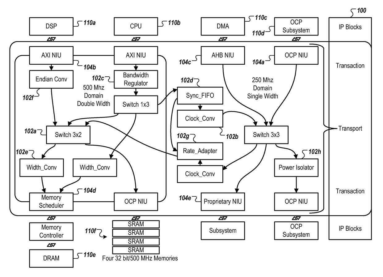
[0021]FIG. 1 is a block diagram of an example NoC 100. In some implementations, NoC 100 can be constructed out of a set of IP elements 102 which communicate with each other through a packet-based transport-protocol. Examples of IP elements 102 include but are not limited to: switches 102a, clock converters 102b, bandwidth regulators 102c, sync First In First Out (FIFO) 102d, width converters 102e, Endian converters 102f, rate adaptors 102g, power isolators 102h and other IP elements.
[0022]In some implementations, at the edges of NoC 100, Network Interface Units (NIUs) 104 implement a conversion between transaction protocol and transport protocol (ingress) and vice versa (egress). Some examples of NIUs for transaction protocols include but are not limited to: OCP NIU 104a, AXI™ NIU 104b, AHB™ NIU 104c, memory scheduler 104d and a proprietary NIU 104e. The NIUs 104 couple to various IP cores 110. Some examples of IP cores are DSP 110a, CPU 110b, Direct Memory Access 110c, OCP subsyste...
example physical
Link
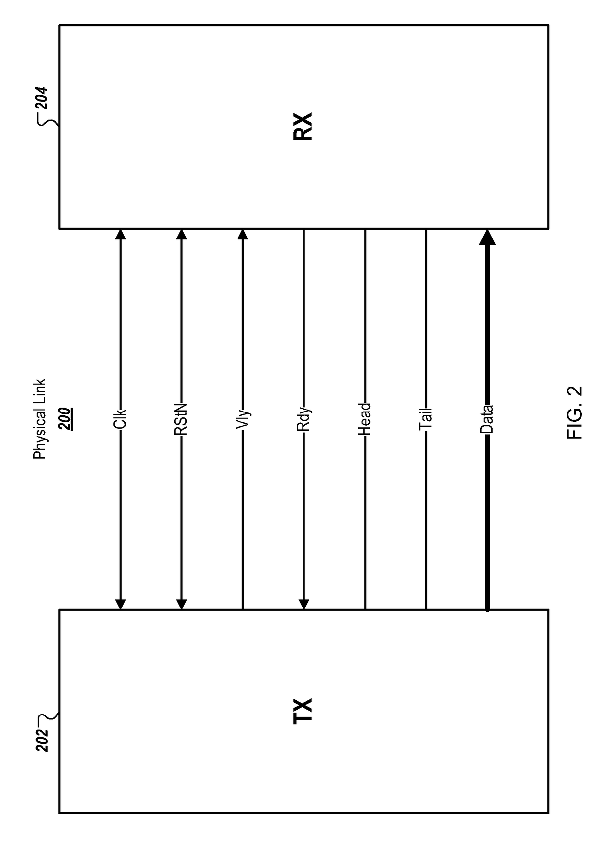
[0024]FIG. 2 is a block diagram of an example physical link 200 connecting a transmitter 202 (TX) and a receiver 204 (RX) in NoC 100 of FIG. 1. A transport protocol socket can be used to transfer a packet from transmitter 202 to receiver 204 over physical link 200. The socket can contain flow control signals (Vld, Rdy), framing signals (Head, Tail) and information signals (Data). The socket can be a synchronous interface working on rising edges of a clock signal (Clk). One active low reset signal (RStN) can also be included in the physical link 200. The logical meaning of the different signals in this particular implementation is described next.[0025]Vld: Indicates that transmitter 202 presents valid information (Head, Tail and Data) in a current clock cycle. When Vld is negated, transmitter 202 drives an X value on Head, Tail and Data and receiver 204 discards these signals. Once transmitter 202 asserts Vld, the signals Head, Tail, Data and Vld remain constant until Rdy is asse...
PUM
 Abstract
Description
Claims
Application Information
 - R&D
- Intellectual Property
- Life Sciences
- Materials
- Tech Scout
- Unparalleled Data Quality
- Higher Quality Content
- 60% Fewer Hallucinations
Browse by: Latest US Patents, China's latest patents, Technical Efficacy Thesaurus, Application Domain, Technology Topic, Popular Technical Reports.
© 2025 PatSnap. All rights reserved.Legal|Privacy policy|Modern Slavery Act Transparency Statement|Sitemap|About US| Contact US: help@patsnap.com