Imaging apparatus and radiographic imaging system
a radiographic imaging and imaging apparatus technology, applied in the field of imaging apparatus and radiographic imaging system, can solve the problem of significantly insufficient settling time of the output amplifier
- Summary
- Abstract
- Description
- Claims
- Application Information
AI Technical Summary
Benefits of technology
Problems solved by technology
Method used
Image

Examples
first embodiment
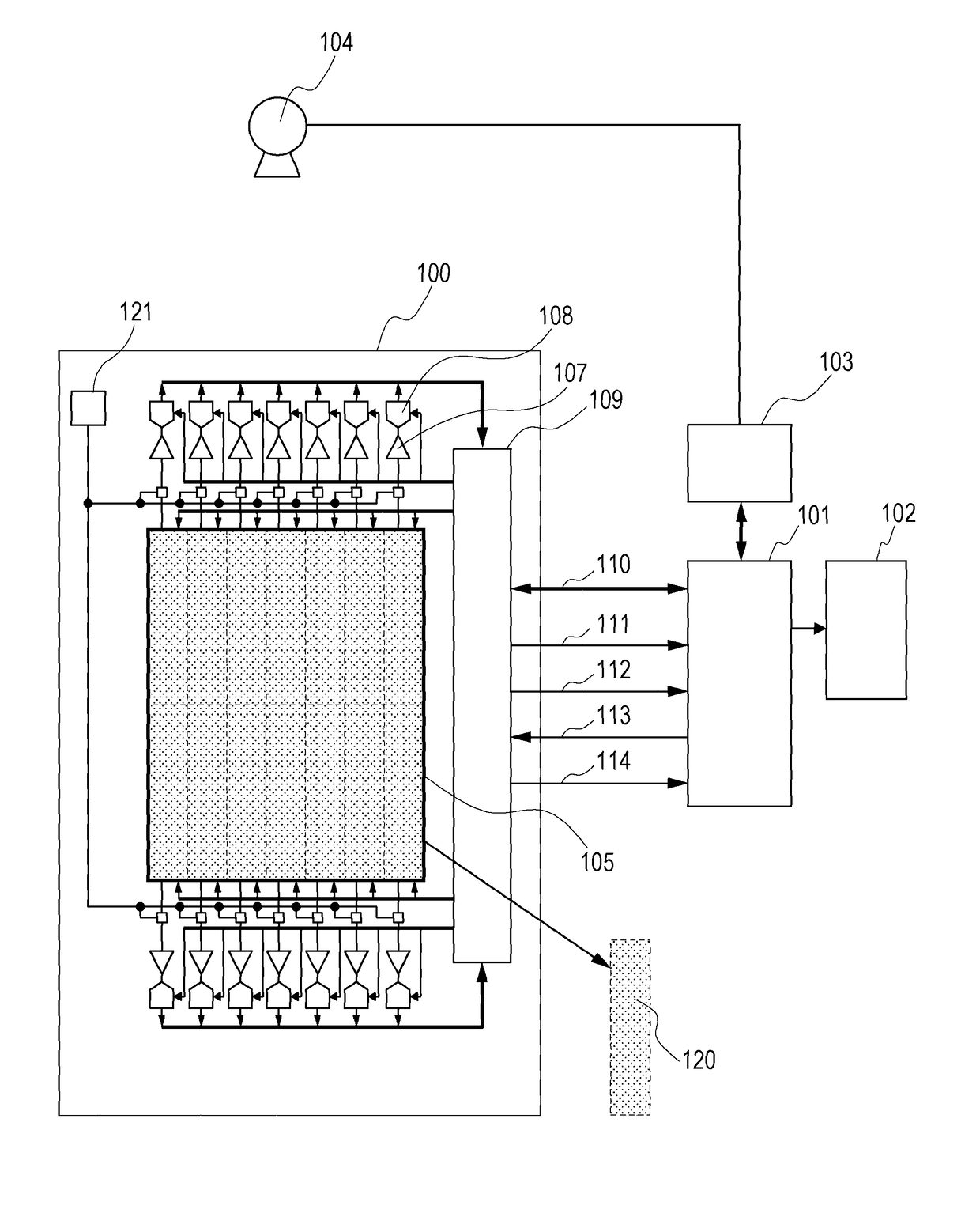
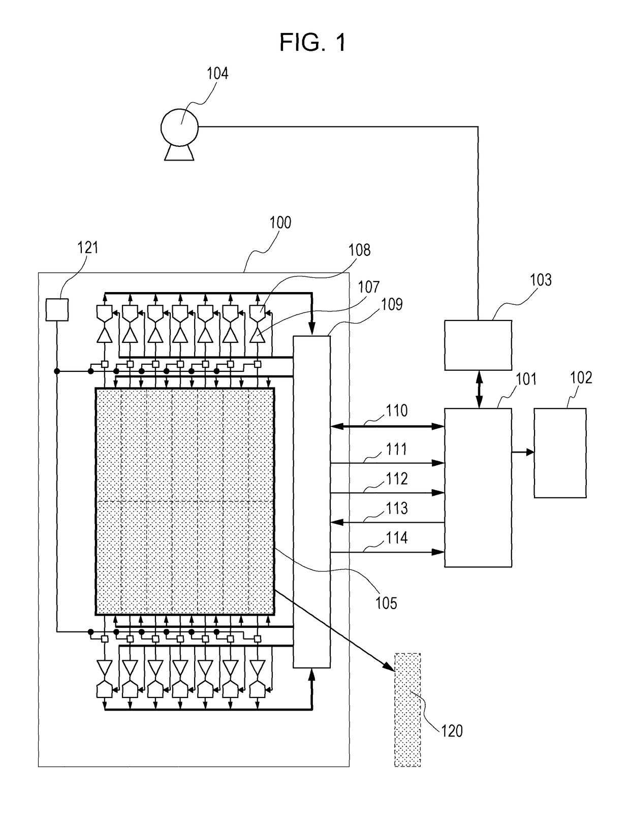
[0025]First, a radiographic imaging system including an imaging apparatus will be described with reference to FIG. 1. FIG. 1 is a schematic block diagram of the radiographic imaging system.
[0026]FIG. 1 illustrates an imaging apparatus 100, an image processing device 101, an image display apparatus 102, an X-ray generator (radiation generator) 103, and an X-ray tube 104. In photographing, a control device (not shown) controls such that the imaging apparatus 100 and the X.-ray generator 103 can synchronize with each other. An X-ray having transmitted through an object is converted to visible light by a scintillator, not illustrated, is photoelectrically converted on the basis of light quantity, and is then A / D converted. After that, the frame image data corresponding to the X-ray irradiation are transferred from the imaging apparatus 100 to the image processing device 101. After the transferred frame image data undergoes image processing, the resulting radiographic image is displayed ...
second embodiment
[0052]Next, a second embodiment will be described with reference to FIGS. 8 to 13. Like numbers refer to like parts in the first and second embodiments, and any repetitive detail description will be omitted. Differences from the first embodiment will mainly be described below.
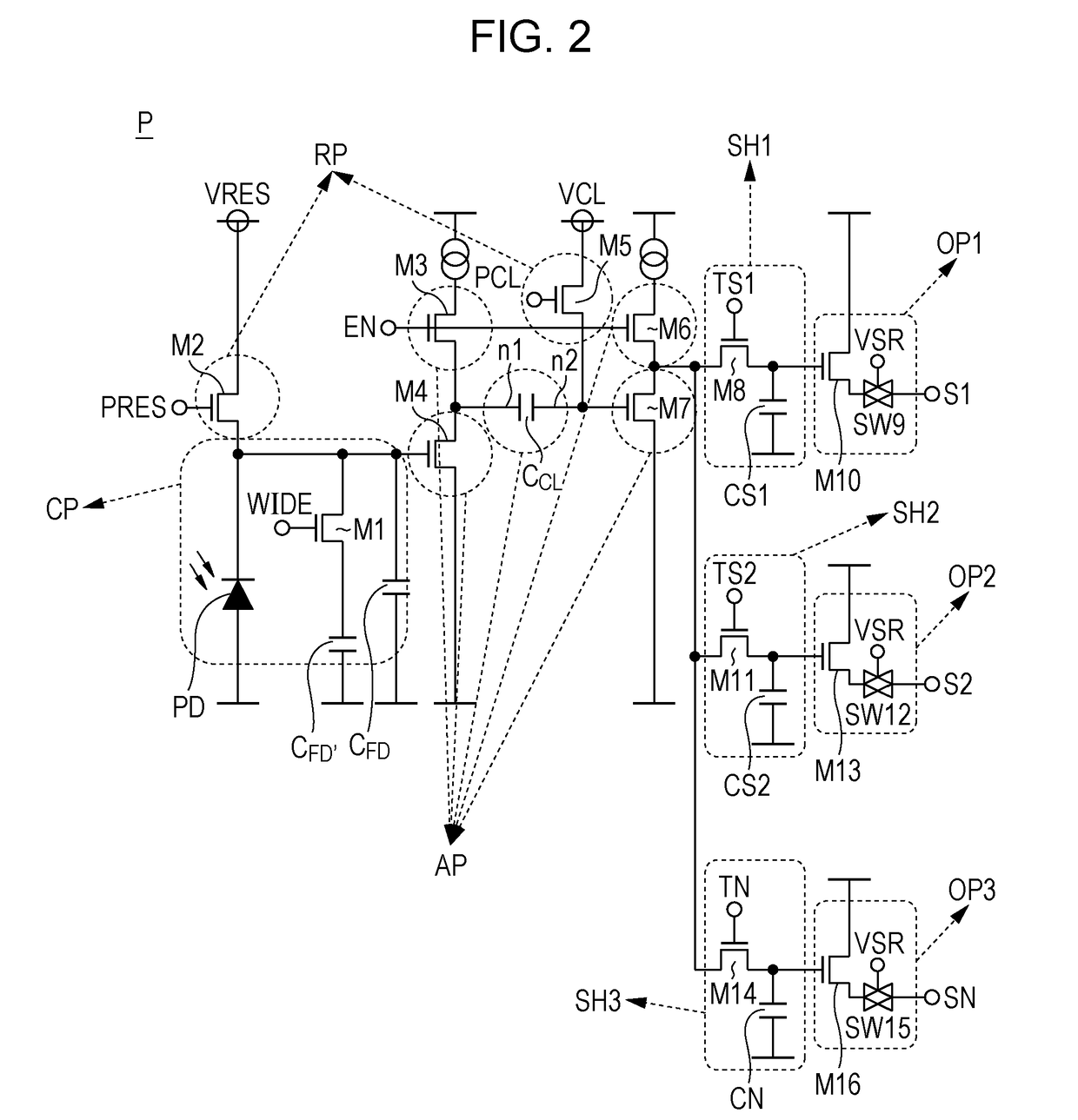
[0053]As illustrated in FIG. 8, the imaging apparatus according to this embodiment further includes a correction unit configured to supply correction voltage to an input of the differential amplifier 107. The correction voltage is usable for correcting offset components in the differential amplifier 107 and the A / D converter 108 based on a digital signal from the A / D converter 108. More specifically, the correction unit includes a D / A converter 131 and an amplifier 132 configured to supply correction voltage based on a correction signal DAIN to an input to the differential amplifier 107. As illustrated in FIG. 9, the D / A converter 131 and the amplifier 132 input the correction voltage to an inverting input term...
third embodiment
[0065]Next, a third embodiment will he described with reference to FIGS. 14 to 16. Like numbers refer to like parts in the first, second and third embodiments, and any repetitive detail descriptions will be omitted. Differences from the second embodiment, will mainly be described below.
[0066]As illustrated in FIG. 14, the third embodiment is different from the second embodiment illustrated in FIG. 10 in that output enabled multiplexers 450 to 452, analog output lines 440 to 442 for odd-numbered columns, and analog output lines 443 to 445 for even-numbered columns are further provided. Each of the analog output lines for odd-numbered columns and even-numbered columns provided in the previous stage of the analog output line 409 to 411 can have a reduced capacitance component. A reference voltage Vref and the analog output lines (409, 410, 411, 440, 441, 442, 443, 444, 445) may be connected through impedance conversion a source follower, for example. Thus, the analog output lines can b...
PUM
 Abstract
Description
Claims
Application Information
 - R&D
- Intellectual Property
- Life Sciences
- Materials
- Tech Scout
- Unparalleled Data Quality
- Higher Quality Content
- 60% Fewer Hallucinations
Browse by: Latest US Patents, China's latest patents, Technical Efficacy Thesaurus, Application Domain, Technology Topic, Popular Technical Reports.
© 2025 PatSnap. All rights reserved.Legal|Privacy policy|Modern Slavery Act Transparency Statement|Sitemap|About US| Contact US: help@patsnap.com