Liquid crystal display and common voltage compensation driving method thereof
a technology of liquid crystal display and driving method, which is applied in the direction of instruments, static indicating devices, etc., can solve the problems of device inoperativeness, voltage drop in the input terminal, heat generation and degradation of other characteristics of the device,
- Summary
- Abstract
- Description
- Claims
- Application Information
AI Technical Summary
Benefits of technology
Problems solved by technology
Method used
Image


Examples
first example embodiment
[0027]FIG. 1 is a block diagram schematically illustrating an example of a liquid crystal display (LCD) device, and FIG. 2 is a circuit diagram schematically illustrating an example of a sub-pixel (SP) as illustrated in FIG. 1.
[0028]As illustrated in FIG. 1, the LCD device includes an image supply unit 120, a timing controller 130, a gate driver 140, a data driver 150, a liquid crystal panel 160, a backlight unit 170, and a power supply unit 180.
[0029]The image supply unit 120 processes a data signal and outputs the data signal together with a vertical synchronization signal, a horizontal synchronization signal, a data enable signal, and a clock signal. The image supply unit 120 supplies the vertical synchronization signal, the horizontal synchronization signal, the data enable signal, the clock signal, and the data signal to the timing controller 130.
[0030]The timing controller 130 generates a gate timing control signal GDC for controlling an operation timing of the gate driver 140...
second example embodiment
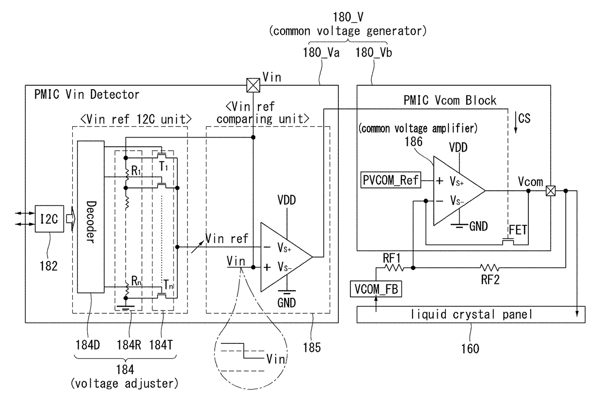
[0074]FIG. 10 is a block diagram illustrating a portion of an example common voltage generating unit according to a second example embodiment of the present disclosure.
[0075]As illustrated in FIG. 10, the common voltage generation unit 180_V includes a first circuit unit 180_Va (PMIC Vin Detector) detecting an input voltage, and a second circuit unit 180_Vb (PMIC Vcom Block) generating a common voltage Vcom.
[0076]The first circuit unit 180_Va outputs a control signal CS for controlling a compensation ratio of the common voltage Vcom output from the second circuit unit 180_Vb on the basis of a signal supplied from an external circuit unit and an input voltage Vin supplied from the outside.
[0077]The first circuit unit 180_Va includes an interface unit 182, a voltage adjusting unit 184, and a voltage comparing unit 185. The interface unit 182 exchanges data with an external circuit unit (hereinafter, referred to as a “timing controller”) according to a communication interface (IF) sche...
third example embodiment
[0096]FIG. 11 is a block diagram illustrating a portion of the common voltage generating unit according to a third example embodiment of the present disclosure.
[0097]As illustrated in FIG. 11, the example common voltage generation unit 180_V includes a first circuit unit 180_Va (PMIC Vin Detector) detecting an input voltage and a second circuit unit 180_Vb (PMIC Vcom Block) generating a common voltage Vcom.
[0098]The first circuit unit 180_Va outputs a control signal CS for controlling a compensation ratio of the common voltage Vcom output from the second circuit unit 180_Vb on the basis of a signal supplied from an external circuit unit and an input voltage Vin supplied from the outside.
[0099]The second circuit unit 180_Vb controls a compensation ratio of the common voltage Vcom in response to the control signal CS supplied from the first circuit unit 180_Va. The second circuit unit 180_Vb includes a common voltage amplifying unit 186 amplifying a common voltage and outputting the a...
PUM
 Abstract
Description
Claims
Application Information