Method for fabricating semiconductor device structure and product thereof

a semiconductor device and structure technology, applied in the field of semiconductor device structure and product thereof, can solve the problems of large variation of breakdown voltage of hv device, and achieve the effect of reducing the variation of breakdown voltage of hv mos devi

Active Publication Date: 2018-03-20
UNITED MICROELECTRONICS CORP
View PDF4 Cites 0 Cited by
  • Summary
  • Abstract
  • Description
  • Claims
  • Application Information

AI Technical Summary

Benefits of technology

[0006]Accordingly, this invention provides a method for fabricating a semiconductor device structure, which is capable of reducing the variation of the breakdown voltage of an HV MOS device.
[0012]As this invention is applied to an HV MOS device, since the portion of the thick gate dielectric layer that is located on the part of the substrate to be formed with the first S / D region therein is removed in advance, the implantation of the first S / D region does not pass through the thick gate dielectric layer, so that the uniformity of the shallow S / D junction is reduced and the variation of breakdown voltage of the HV device is reduced.

Problems solved by technology

However, the thick gate oxide layer is so thick that the uniformity of the shallow source / drain (S / D) junction formed by ion implantation through the gate oxide layer is reduced, so that the variation of breakdown voltage of the HV device is large.

Method used


Image

  • Method for fabricating semiconductor device structure and product thereof
  • Method for fabricating semiconductor device structure and product thereof
  • Method for fabricating semiconductor device structure and product thereof

Examples


Embodiment Construction

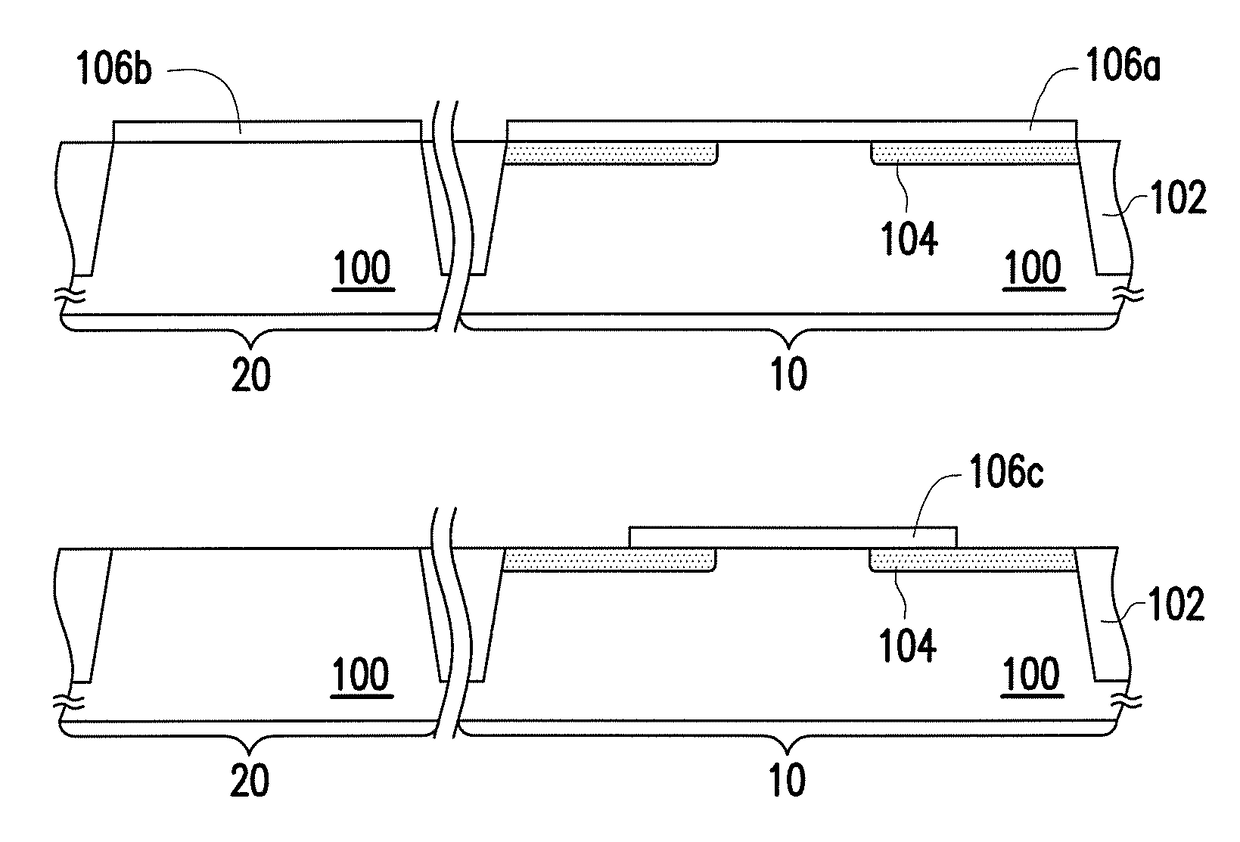
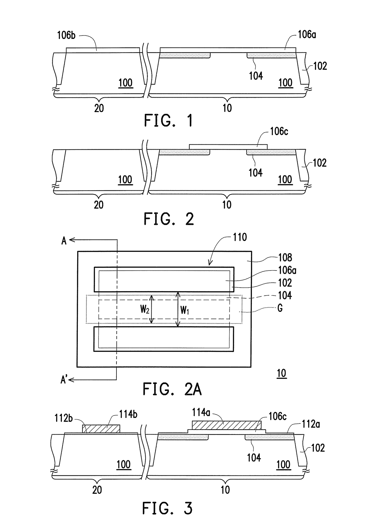
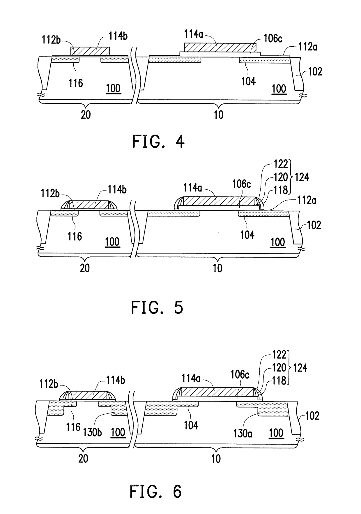
[0016]This invention will be further explained with the following embodiment and the accompanying drawings, which are not intended to restrict the scope of this invention. For example, although in the illustrated embodiment the first MOS device is an HV device that is formed simultaneously with a second MOS device being an LV device, this invention can also be applied to a case where the first MOS device is another kind of MOS device whose gate dielectric layer would affect the uniformity of the S / D junctions thereof, or a case forming only HV devices.

[0017]FIGS. 1, 2, 3, 4, 5 and 6 illustrate, in a cross-sectional view, a method for fabricating a semiconductor device structure according to an embodiment of this invention, wherein FIG. 6 also illustrates the structure of the semiconductor device structure according to the embodiment. FIG. 2A illustrates, in a top view, a local structure of the patterned mask layer used in the step illustrated in FIG. 2, wherein the local structure i...


PUM


Abstract

A method for fabricating a semiconductor device structure is shown. A gate dielectric layer is formed on a substrate. A portion of the gate dielectric layer, which is located on a part of the substrate in which an S / D region is to be formed, is removed. A gate electrode is formed on the remaining gate dielectric layer. A spacer is formed on the sidewall of the gate electrode and the sidewall of the gate dielectric layer. The S / D region is then formed in the part of the substrate beside the spacer.

Description

BACKGROUND OF THE INVENTION[0001]Field of Invention[0002]This invention relates to a semiconductor process, and particularly relates to a method for fabricating a semiconductor device structure, and to a semiconductor device structure that can be formed with the same method.[0003]Description of Related Art[0004]Some kinds of integrated circuits include high-voltage (HV) MOS devices, such as Input / Output (I / O) devices, for high-voltage operations. Since the operation voltage is high, an HV device requires a thick gate oxide layer.[0005]However, the thick gate oxide layer is so thick that the uniformity of the shallow source / drain (S / D) junction formed by ion implantation through the gate oxide layer is reduced, so that the variation of breakdown voltage of the HV device is large.SUMMARY OF THE INVENTION[0006]Accordingly, this invention provides a method for fabricating a semiconductor device structure, which is capable of reducing the variation of the breakdown voltage of an HV MOS d...

Claims


Application Information

Patent Timeline
Patent Type & Authority Patents(United States)
IPC IPC(8): H01L21/8234H01L29/08H01L27/092H01L29/423H01L27/088
CPCH01L21/823462H01L21/823418H01L21/823437H01L29/42364H01L27/0922H01L29/0847H01L27/088H01L29/7836
Inventor CHANG, KAI-KUENHSIAO, SHIH-YIN
Owner UNITED MICROELECTRONICS CORP
Why Eureka
Try Eureka