Image sensor

a technology of image sensor and substrate, applied in the field of image sensor, can solve the problems of deteriorating reliability of image sensor, reducing the efficiency of charge collection, and inefficient use of resources and time, so as to avoid delamination or cracking of the photoconductive layer, reduce thermal stress between the photoconductive layer and the substrate, and reduce the effect of thermal stress

Active Publication Date: 2018-03-20
RAYENCE +1
View PDF1 Cites 0 Cited by
  • Summary
  • Abstract
  • Description
  • Claims
  • Application Information

AI Technical Summary

Benefits of technology

[0011]Accordingly, the present invention has been made keeping in mind the above problems occurring in the related art, and the present invention is to propose a way to increase the strength of adhesion between a photoconductive layer and a substrate and thus reliability of an image sensor is ensured.
[0019]Accordingly, thermal stress between the photoconductive layer and the substrate is reduced, so the strength of adhesion therebetween is increased and defects such as delamination or cracking of the photoconductive layer may be avoided. Thus, reliability of the image sensor is improved since current leakage of the photoconductive layer is reduced.
[0021]Therefore, according to the present invention, thermal stress between the photoconductive layer and the substrate is reduced, so the strength of adhesion of the photoconductive layer relative to the substrate is increased and defects such as delamination or cracking of the photoconductive layer may be avoided. Thus, charge collection efficiency of the image sensor is increased and current leakage of the photoconductive layer is reduced, thus improving operational reliability of the image sensor element.

Problems solved by technology

In this case, the use of resources and time becomes inefficient due to problems related to the development and storage of the taken films.
Accordingly, reliability of image sensors is deteriorated since current leakage increases due to the delamination or the cracking of the photoconductive layer and thus charge collection efficiency is degraded.

Method used


Image

  • Image sensor
  • Image sensor
  • Image sensor

Examples


Embodiment Construction

[0025]Hereinbelow, exemplary embodiments of the present invention will be described in detail with reference to the accompanying drawings.

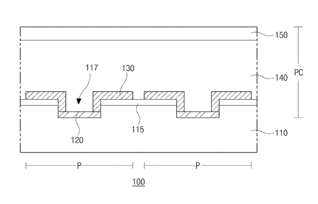
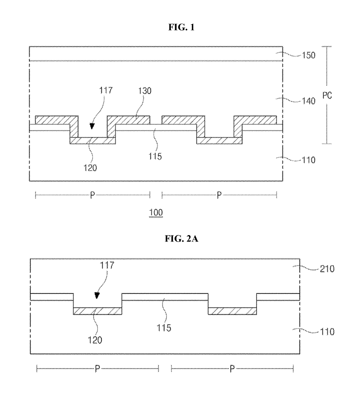
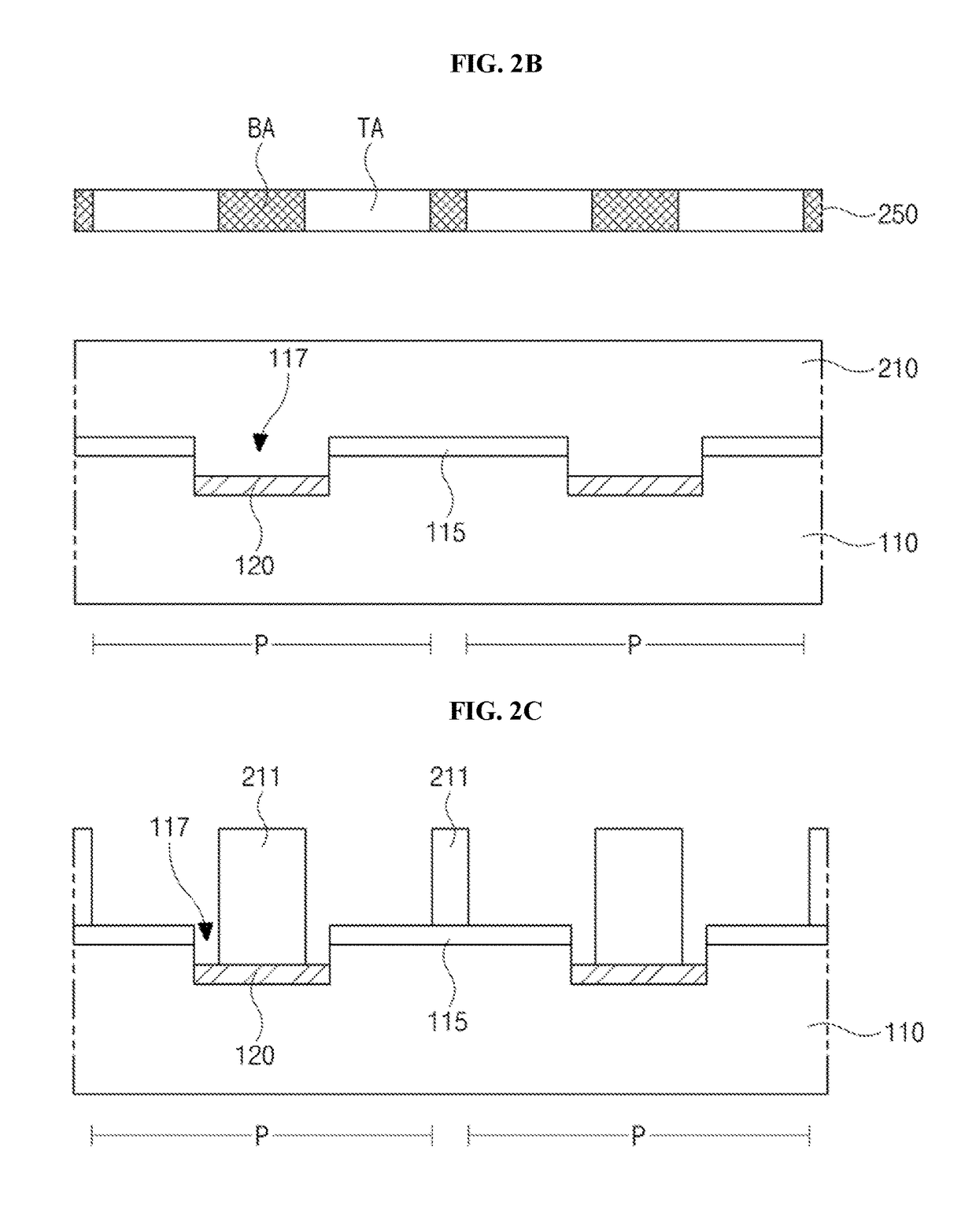
[0026]FIG. 1 is a cross-sectional view schematically showing an image sensor according to an embodiment of the present invention.

[0027]An image sensor 100 according to an embodiment of the present invention may be used in a variety of X-ray imaging devices having various shapes or end uses. For example, the X-ray imaging devices may include mammographic devices, CT devices, etc.

[0028]The image sensor 100 corresponds to a configuration in which X-rays that have passed through a target are detected and then converted into an electrical signal. The image sensor 100 has a rectangular shape when viewed from above, but it is not limited thereto.

[0029]In particular, the image sensor 100 according to the embodiment of the present invention is a direct conversion-type X-ray detector, in which incident X-rays are directly converted into an electrical signal...


PUM


Abstract

There is provided an image sensor including: a plurality of first electrodes respectively formed within a plurality of pixel areas, the pixel areas being formed on a substrate; a protection layer formed on an upper surface of the substrate and including a plurality of contact holes respectively exposing the first electrodes of the pixel areas; a plurality of auxiliary electrodes respectively contacting with the first electrodes through the contact holes and extending to an upper surface of the protection layer of the pixel area; a photoconductive layer formed on both the first electrodes and on the auxiliary electrodes; and a second electrode formed on the photo conductive layer.

Description

CROSS REFERENCE TO RELATED APPLICATION[0001]The present application claims priority to Korean Patent Application No. 10-2016-0001775, filed Jan. 6, 2016, the entire contents of which is incorporated herein for all purposes by this reference.BACKGROUND OF THE INVENTION[0002]Field of the Invention[0003]The present invention generally relates to an image sensor and manufacturing method thereof. More particularly, the present invention relates to an image sensor in which the strength of adhesion between a photoconductive layer and a substrate is increased.[0004]Description of the Related Art[0005]Conventionally, X-rays for medical or industrial applications have typically used films and screens. In this case, the use of resources and time becomes inefficient due to problems related to the development and storage of the taken films.[0006]Hence, digital-type image sensors are currently widely used. Such image sensors are classified into: indirect conversion-type image sensors and direct c...

Claims


Application Information

Patent Timeline
Patent Type & Authority Patents(United States)
IPC IPC(8): H01L27/00H01L27/146H01L31/0224H01L29/47
CPCH01L27/14685H01L27/14603H01L27/14676H01L31/0224H01L27/14609H01L29/47H01L31/115
Inventor KIM, KI HYUNGKIM, TAE WOOLEE, DONG JIN
Owner RAYENCE
Why Eureka
Try Eureka