Switched mode negative inductor

a negative inductor and switch mode technology, applied in the field of circuit synthesis, can solve the problems of inconvenient use, inconvenient operation, and inability to achieve full-size antennas on mobile platforms such as aircra

Active Publication Date: 2018-03-20
HRL LAB
View PDF9 Cites 0 Cited by
  • Summary
  • Abstract
  • Description
  • Claims
  • Application Information

AI Technical Summary

Benefits of technology

[0019]Certain embodiments may provide various technical advantages depending on the implementation. For example, a technical advantage of some embodim

Problems solved by technology

However, full size antennas are often times not feasible on mobile platforms such as aircraft.
The disadvantage is that it results in an extremely narrowband performance for high-Q loads, such as compact antennas, and is not useful if wideband performance is required.
In addition, performance outside the band of interest results in extremely poor performance.
This approach has extremely low power efficiency.
Large and expensive power amplifiers and cooling systems are needed to generate and dissipate RF power.
The unmatched case complicates amplifier design because it must handle reflected power, while lossy matching further reduces efficiency.
Such use does not extend to high power levels due

Method used


Image

  • Switched mode negative inductor
  • Switched mode negative inductor
  • Switched mode negative inductor

Examples


Embodiment Construction

[0026]It should be understood at the outset that, although example embodiments are illustrated below, the present invention may be implemented using any number of techniques, whether currently known or not. The present invention should in no way be limited to the example implementations, drawings, and techniques illustrated below. Additionally, the drawings are not necessarily drawn to scale.

[0027]The principles of this invention is the synthesis of negative inductance circuits that can provide for efficient high power and broad band performance. Negative inductance can be illustrated by the following equation:

[0028]d⁢⁢Id⁢⁢t=VL<0(1)

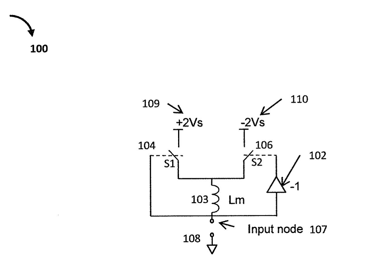
[0029]where I is the current through the device, t is time, V is the voltage across the terminals and L<0 is the inductance.

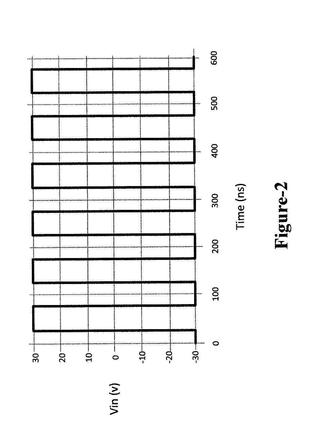
[0030]An embodiment of the present invention is a circuit that synthesizes a negative inductance in a switching mode. In an embodiment of this inventive concept, the negative inductance behavior is observed when driven by a voltag...


PUM


Abstract

A switched mode negative inductance circuit includes an input node responsive to a voltage signal. The circuit also includes first and second voltage sources, first and second controlled switches having first poles coupled to the first and second voltage sources, respectively and an inductor having a first electrode coupled to second poles of the first and second controlled switches and a second electrode coupled to the input node. The input node is coupled to a control electrode of the first controlled switch, and to a control electrode of the second controlled switch through a voltage inverting circuit. The disclosure also illustrates balanced negative inductance circuits and implementation approaches using NMOS transistors.

Description

CROSS REFERENCE TO RELATED APPLICATIONS[0001]This application claims the benefit of U.S. Provisional Patent Application No. 62 / 146,964, filed Apr. 14, 2015, which is incorporated herein by reference in its entirety.TECHNICAL FIELD[0002]The present invention is in the field of circuit synthesis and in particular relates to a circuit that synthesizes a negative inductance.BACKGROUND OF THE DISCLOSURE[0003]There are a variety of applications where canceling inductive reactance over a wide frequency bands are required. Such applications can benefit from negative inductance circuits to offset the inductive reactance and provide for efficient power transfers. Examples of such applications include systems with small transmit antennas, and in particular to antennas at and below VHF frequencies. In order to operate efficiently, antennas must be matched to the transmitting circuitry.[0004]Large antennas are more easily matched because they operate at a relatively low Q factor. However, full s...

Claims


Application Information

Patent Timeline
IPC IPC(8): H03H11/48H03H11/10
CPCH03H11/48H03H11/10
Inventor WHITE, CARSON R.HUGHES, BRIAN
Owner HRL LAB
Why Eureka
Try Eureka