Solid-state lighting structure with light modulation control

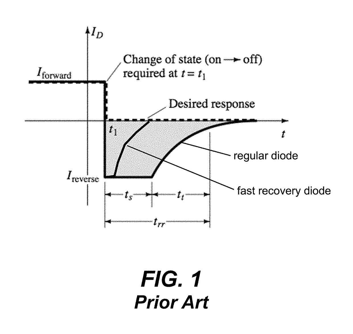
a lighting structure and solid-state technology, applied in the field of solid-state lighting structures, can solve the problems of protracted light turn-off time of deep uv leds, and relatively long recombination time of electrons and holes

Active Publication Date: 2018-04-17
SENSOR ELECTRONICS TECH
View PDF7 Cites 1 Cited by
  • Summary
  • Abstract
  • Description
  • Claims
  • Application Information

AI Technical Summary

Benefits of technology

[0007]Aspects of the present invention are directed to improving the light modulation of SSLSs, e.g., by attaining faster on / off switching times, and thus, improved performance of the SSLSs. In one embodiment, a device can include an SSLS having a main p-n junction region configured for recombination of electron-hole pairs for light emission, and at least one supplementary p-n junction region proximate the main p-n junction region to supplement the recombination of electron-hole pairs. The supplementary p-n junction region can supplement the recombination of electron-hole pairs by redirecting the electron-hole flow direction away from the light generating structure of the device, which leads to faster light turn-off. In addition, the supplementary p-n junction region can have a smaller electron-hole life time than the electron-hole life time of the main p-n junction region, which also leads to faster light turn-off. In one embodiment, the electron-hole life time of the supplementary p-n junction region is 10 to 100 times smaller than the electron-hole life time of the main p-n junction region. The main p-n junction region and the supplementary p-n junction region can operate cooperatively in a light emission state and a light turn-off-state. In one embodiment, the recombination of electron-hole pairs can occur in the main p-n junction region during the light emission state, and the recombination of electron-hole pairs can occur in the supplementary p-n junction region during the light turn off-state.
[0008]A pair of main electrodes can be formed over the main p-n junction region and a supplementary electrode can be formed over the supplementary p-n junction region. In one embodiment, the pair of main electrodes and the main p-n junction region can form a main current path, while the supplementary electrode and one of the main electrodes along with the supplementary p-n junction region can form a current redirection path. A bias can be applied through either the main current path to the main p-n junction region or the current redirection path to the supplementary p-n junction region. For example, the bias can be applied through the main current path to the main p-n junction region in a light emission state, while the bias can be applied through the current redirection path to the supplementary p-n junction region in a light turn-off state. Because the supplementary p-n junction region can have a smaller electron-hole life time than the main p-n junction region, the recombination of pairs of electrons and holes occurs faster. This enables the supplementary p-n junction region to have a faster light modulation, and thus, is well suited for use in the light turn-off state as opposed to the main p-n junction region which is more suitable for use in the light emission state.

Problems solved by technology

A piezoelectric effect, certain type of traps, and other factors associated with the LEDs, cause the recombination of electron and holes to take a relatively long time after a pumping current has been shut off.
A longer recombination of electrons and holes after the pumping current has been shut off translates into a protracted light turn-off time.
Deep UV LEDs can also have a relatively long light turn-off time due to the recombination of electrons and holes.
However, this approach inevitably results in lower light emission and lower LED efficiency.
However, modulation with an external light modulator involves additional optical loss, power consumption, and leads to significant increase in the overall size, weight and cost of the SSLS devices.

Method used


Image

  • Solid-state lighting structure with light modulation control
  • Solid-state lighting structure with light modulation control
  • Solid-state lighting structure with light modulation control

Examples


Embodiment Construction

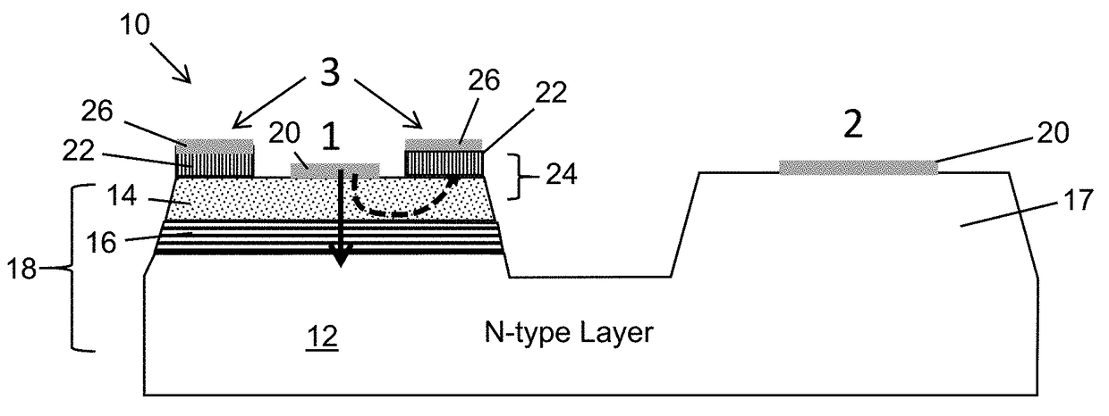
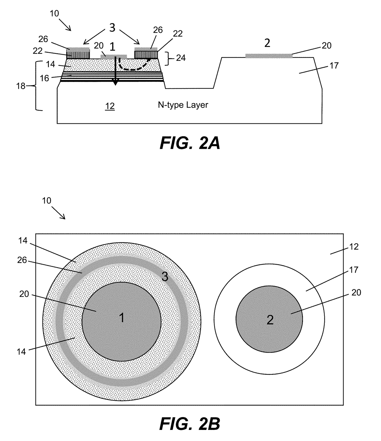
[0028]The various embodiments are directed to SSLSs with light modulation control to attain faster on / off switching times. In one embodiment, an SSLS can have a main p-n junction region for recombination of electron-hole pairs for light emission and a supplementary p-n junction region proximate the main p-n junction region to supplement the recombination of electron-hole pairs. The supplementary p-n junction region can have a smaller electron-hole life time than the electron-hole life time of the main p-n junction region. In addition, the supplementary p-n junction region can serve to redirect the electron-hole flow direction away from the light generating structure of the device. With this configuration, the main p-n junction region and the supplementary p-n junction region can operate cooperatively in a light emission state and a light turn-off-state for faster light modulation. In one embodiment, the recombination of electron-hole pairs can occur in the main p-n junction region d...


PUM


Abstract

A solid-state light source (SSLS) with light modulation control is described. A SSLS device can include a main p-n junction region configured for recombination of electron-hole pairs for light emission. A supplementary p-n junction region is proximate the main p-n junction region to supplement the recombination of electron-hole pairs, wherein the supplementary p-n junction region has a smaller electron-hole life time than the electron-hole life time of the main p-n junction region. The main p-n junction region and the supplementary p-n junction region operate cooperatively in a light emission state and a light turn-off-state. In one embodiment, the recombination of electron-hole pairs occurs in the main p-n junction region during a light emission state, and the recombination of electron-hole pairs occurs in the supplementary p-n junction region light during the light turn off-state.

Description

REFERENCE TO RELATED APPLICATIONS[0001]The present patent application claims the benefit of U.S. Provisional Application No. 62 / 218,073, which was filed on 14 Sep. 2015, and which is hereby incorporated by reference.TECHNICAL FIELD[0002]The present invention relates generally to solid-state lighting, and more particularly, to solid-state lighting structures (SSLSs), such as light emitting diodes (LEDs) and lasers, with light modulation control that enables a faster on / off switching time.BACKGROUND ART[0003]A great deal of interest has been focused on SSLSs, such as LEDs and lasers, and in particular, those that emit light in the blue and deep ultraviolet (UV) wavelengths. These devices may be capable of being incorporated into various applications, including solid-state lighting, biochemical disinfection and detection, high-density data storage, and the like.[0004]Modern SSLSs, such as an LEDs, typically include three major components: an electron supply layer (e.g., an n-type semic...

Claims


Application Information

Patent Timeline
Patent Type & Authority Patents(United States)
IPC IPC(8): H01L33/00H01S5/042H01L33/36H01L33/14H01S5/06H01L33/20H01S5/062H01L33/38H01L33/32H01L33/08H01S5/343H05B44/00
CPCH01S5/062H01L33/0004H01L33/14H01L33/20H01L33/36H01L33/38H01S5/0602H01S5/06203H01S5/0421H01S5/34333H01L33/08H01L33/32H01S5/0427
Inventor SIMIN, GRIGORYSHUR, MICHAEL
Owner SENSOR ELECTRONICS TECH
Why Eureka
Try Eureka