
Curved grating structure manufacturing method, curved grating structure, grating unit, and x-ray imaging device

a technology of curved grating and manufacturing method, which is applied in the direction of radiation generation arrangement, instruments, applications, etc., can solve the problems of insufficient curvature, more likely to break the mold during manufacturing, and insufficient curvature, and achieves small curvature radius and high handleability.

Active Publication Date: 2018-05-15
KONICA MINOLTA INC
View PDF12 Cites 18 Cited by
  • Summary
  • Abstract
  • Description
  • Claims
  • Application Information

AI Technical Summary

Problems solved by technology

Meanwhile, in the microstructural body manufacturing method disclosed in the Patent Literature 1, when the mold is curved by the stress arising from the second plated layer, an excessively large thickness of the mold can cause an insufficient curvature.
On the other hand, if a thin mold easy to be curved is employed, or the mold is thinned by polishing or the like before forming the second plated layer, in order to obtain a sufficient curvature, a problem such as breaking (crack) of the mold during manufacturing is more likely to occur.
Further, in a situation where the mold is insufficiently curved due to an excessively large thickness thereof, it is conceivable to thin (reduce a thickness of) the insufficiently-curved mold by polishing to thereby allow the mold to become largely curved.
However, this is not realistic because of difficulty in realizing desirable polishing.
In such a manufacturing method using a stress layer such as the second plated layer, there is difficulty in manufacturing a grating structure largely (steeply) curved with a relatively small curvature radius, or a problem during manufacturing, such as crack of a grating structure during manufacturing, is more likely to occur.

Method used


Image

  • Curved grating structure manufacturing method, curved grating structure, grating unit, and x-ray imaging device
  • Curved grating structure manufacturing method, curved grating structure, grating unit, and x-ray imaging device
  • Curved grating structure manufacturing method, curved grating structure, grating unit, and x-ray imaging device

Examples


first embodiment

tructure

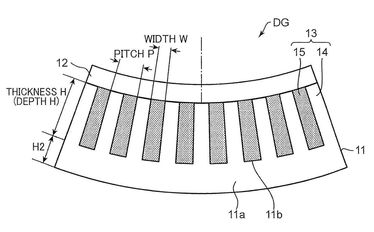
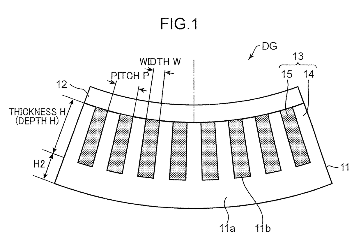
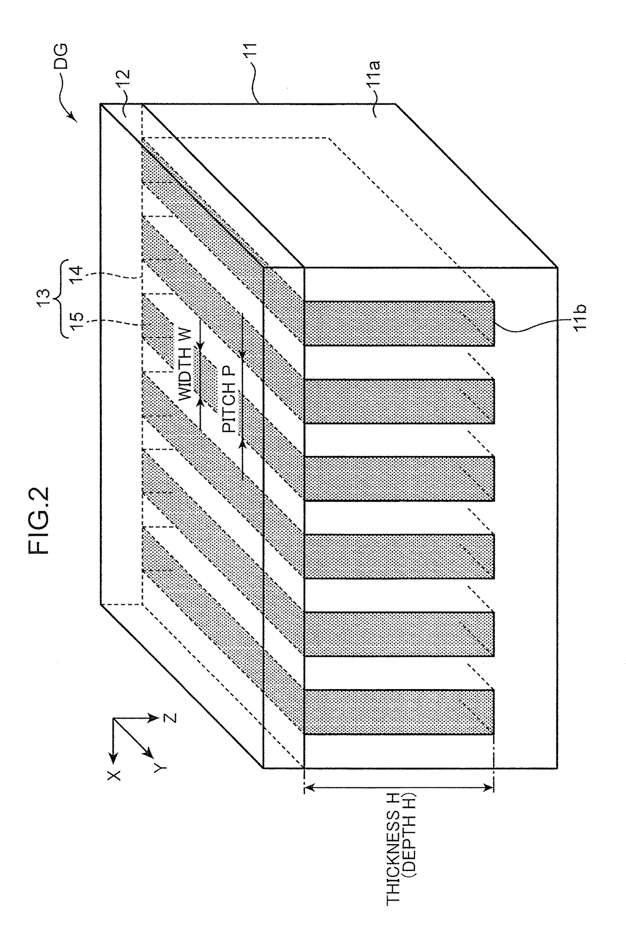
[0032]FIG. 1 is a sectional view depicting a configuration of a curved grating structure according to a first embodiment of the present invention. FIG. 2 is a perspective view depicting the configuration of the curved grating structure according to the first embodiment. In FIG. 2, for the sake of illustration, an aftermentioned grating-forming workpiece 11 and an aftermentioned stress layer 12 are depicted in a flat state without being curved by stress. Actually, the grating-forming workpiece 11 and the stress layer 12 in an aftermentioned curved grating structure DG are curved by a stress, as depicted in FIG. 1.

[0033]As depicted in FIGS. 1 and 2, a curved grating structure DG according to the first embodiment comprises: a grating-forming workpiece 11 as a base material; a grating region 13 formed in one surface (one principal surface) of the grating-forming workpiece 11; and a stress layer 12 formed on a surface of the grating region (grating plane). It should be noted that...

second embodiment

; Grating Unit

[0119]In many cases, a curved grating structure DG is manufactured using a silicon wafer (silicon substrate) capable of being fabricated using microfabrication techniques which have been almost established, as mentioned above. From a viewpoint of easiness in sourcing, sourcing cost and others, the silicon wafer is preferably a commonly-used 6 inch-diameter (φ6 inch) type. A curved grating structure DG fabricatable from such a 6 inch-diameter slicing wafer has a square shape, about 10 cm on a side (□ about 10 cm), and a grating area of □ 10 cm or less. A grating unit DGU according to the second embodiment is directed to resolving restrictions on the grating area.

[0120]FIG. 13 is a diagram depicting a configuration of the grating unit according to the second embodiment. In FIG. 13, for the sake of illustration, each of the curved grating structures DG is depicted in a flat state without being curved. Actually, as depicted in FIG. 1, each of the curved grating structures ...

third and fourth embodiments

lbot-Lau Interferometer

[0125]As an example of application of the above curved grating structure DG and grating unit DGU, they can be suitably used in an X-ray Talbot interferometer and a Talbot-Lau interferometer. In a refraction grating used in an X-ray Talbot interferometer or Talbot-Lau interferometer, it is necessary that a plurality of structural portions are periodically provided with a period of several μm to several ten μm. For this reason, the manufacturing method for the curved grating structure DG according to the first embodiment (including any modification thereof) is suitable for manufacturing of a metal grating structure used in an X-ray Talbot interferometer or Talbot-Lau interferometer having such micro-sized periodical structural portions. The following description will be made about an X-ray Talbot interferometer or Talbot-Lau interferometer using a curved grating structure DG manufactured by the above manufacturing method, or the grating unit DGU according to the...


PUM

PropertyMeasurementUnit
transmittanceaaaaaaaaaa
thicknessaaaaaaaaaa
thicknessaaaaaaaaaa

Abstract

In one aspect, the present invention provides a curved grating structure manufacturing method which comprises: a grating forming step of forming, in one surface of a grating-forming workpiece, a grating region in which a plurality of members mutually having the same shape are periodically provided; a stress layer forming step of forming a stress layer capable of generating stress, on a grating plane-defining surface of the grating region; a boding step of bonding a support substrate to the stress layer; a polishing step of polishing the other surface of the grating-forming workpiece on a side opposite to the one surface having the support substrate bonded thereto; and a peeling step of peeling off the support substrate from the stress layer, wherein the polishing step includes performing the polishing to allow the grating-forming workpiece to be curved by a stress arising from the stress layer, after the peeling step.

Description

RELATED APPLICATIONS[0001]This is a U.S. National Phase Application under 35 USC 371 of International Application PCT / JP2014 / 076460 filed on Oct. 2, 2014.[0002]This application claims the priority of Japanese application no. 2013-221986 filed Oct. 25, 2013, the entire content of which is hereby incorporated by reference.TECHNICAL FIELD[0003]The present invention relates to a manufacturing method for a curved grating structure having a curved-shaped periodic structure, and a curved grating structure manufactured by the manufacturing method. The present invention also relates to a grating unit constructed by arranging a plurality of the curved grating structures side-by-side, and an X-ray imaging device using the curved grating structure.BACKGROUND ART[0004]A diffraction grating is utilized in optical systems of various devices, as a spectral element having a periodic structure composed of a large number of parallel members, and, in recent years, its application to X-ray imaging devic...

Claims


Application Information

Patent Timeline
Patent Type & Authority Patents(United States)
IPC IPC(8): A61B6/00C25D7/00C25D7/12G01T7/00G02B5/18G21K1/06C25D5/10C25D5/48G01N23/205C25D5/02G01N23/00C25D1/00A61B6/06
CPCC25D1/00A61B6/40C25D1/003C25D5/02C25D5/10C25D5/48C25D7/00C25D7/12G01N23/205G01T7/00G02B5/18G02B5/1838G02B5/1857G21K1/06A61B6/00G21K2207/005A61B6/06A61B6/484
Inventor YOKOYAMA, MITSURU
Owner KONICA MINOLTA INC
Learn More