Supercharge Your Innovation With Domain-Expert AI Agents!

Non-volatile memory device

a non-volatile memory and memory device technology, applied in the field of semiconductor memory devices, can solve the problems of insufficient security of the read margin of the threshold voltage state distribution, gradual increase of read errors, and inability to read data, so as to reduce (or minimize) the error bits of the readout page data, the reliability of the operation of the non-volatile memory device may be improved, and the work processing speed.

Active Publication Date: 2018-05-15
THE AIO
View PDF12 Cites 1 Cited by
  • Summary
  • Abstract
  • Description
  • Claims
  • Application Information

AI Technical Summary

Benefits of technology

This approach improves processing speed and reliability by determining an optimal read voltage that reduces error bits, enhancing the operational efficiency of the non-volatile memory device.

Problems solved by technology

A read margin of a threshold voltage state distribution is not sufficiently secured when the MLC NAND flash memory performs the read operation of page data, on that read errors occur.
Further, the read errors may gradually increase due to the threshold voltage state distribution becomes broader with the passage of time.
Therefore, the typical MLC NAND flash memory device is difficult to operate at a high speed.

Method used


Image

  • Non-volatile memory device
  • Non-volatile memory device
  • Non-volatile memory device

Examples


Embodiment Construction

[0026]Exemplary embodiments will be described more fully hereinafter with reference to the accompanying drawings, in which various embodiments are shown.

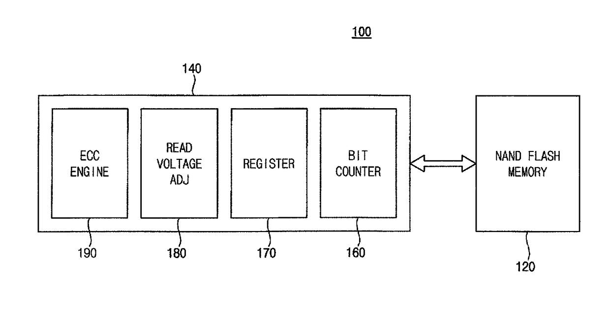
[0027]FIG. 1 is a block diagram of a non-volatile memory device according to example embodiments.

[0028]Referring to FIG. 1, the non-volatile memory device 100 may include a NAND flash memory 120 and a memory controller 140. It should be understood that the non-volatile memory device 100 includes at least one NAND flash memory 120.

[0029]The NAND flash memory 120 may perform a read operation and a write operation to data (hereinafter, page data) by a page unit, and the NAND flash memory performs an erase operation by a block unit. The NAND flash memory 120 may include a memory cell array having a plurality of single level cells (SLCs) or a plurality of multi level cells (MLCs), and a page buffer. The NAND flash memory 120 may interact with the memory controller 140 based on a NAND interface protocol.

[0030]The memory controller 140 may...


PUM


Abstract

A non-volatile memory device according to example embodiments includes at least one NAND flash memory and a memory controller configured to control the NAND flash memory. The memory controller comprises a bit counter configured to count a number of first binary digit of each of first to N-th readout page data, the first to N-th readout page data being respectively read by first to N-th test read voltages, a register configured to store first to N-th count values with respect to the first to N-th readout page data output from the bit counter, and a read voltage adjuster configured to compare the first to N-th count values to determine a read voltage, where N is an integer greater than 1.

Description

BACKGROUND[0001]1. Technical Field[0002]Example embodiments of the inventive concept relate to semiconductor memory devices. More particularly, example embodiments of the inventive concept relate to non-volatile memory devices having multi level cells.[0003]2. Discussion of Related Art[0004]A semiconductor memory device may be classified into tow types (i.e., a volatile memory device and a non-volatile memory device) according to whether data can be retained when power is not supplied. Recently, a NAND flash memory device having multi level cells (Hereinafter, a MLC NAND flash memory device) is widely used as the non-volatile memory device because the NAND flash memory device can be manufactured smaller in size while having higher capacity.[0005]The NAND flash memory device performs a write operation and a read operation by a page unit. A read margin of a threshold voltage state distribution is not sufficiently secured when the MLC NAND flash memory performs the read operation of pa...

Claims


Application Information

Patent Timeline
Patent Type & Authority Patents(United States)
IPC IPC(8): G06F11/00G11C16/34G11C29/02G06F11/10G11C11/56G11C16/26
CPCG11C11/5642G06F11/1044G06F11/1048G06F11/1068G11C29/028G11C16/26G11C16/3404G11C29/021G11C11/5628
Inventor HAN, SEUNG-HYUNHWANG, SUN-MO
Owner THE AIO
Features
  • R&D
  • Intellectual Property
  • Life Sciences
  • Materials
  • Tech Scout
  • Unparalleled Data Quality
  • Higher Quality Content
  • 60% Fewer Hallucinations
Learn More