
Semiconductor device, electronic component, and electronic device

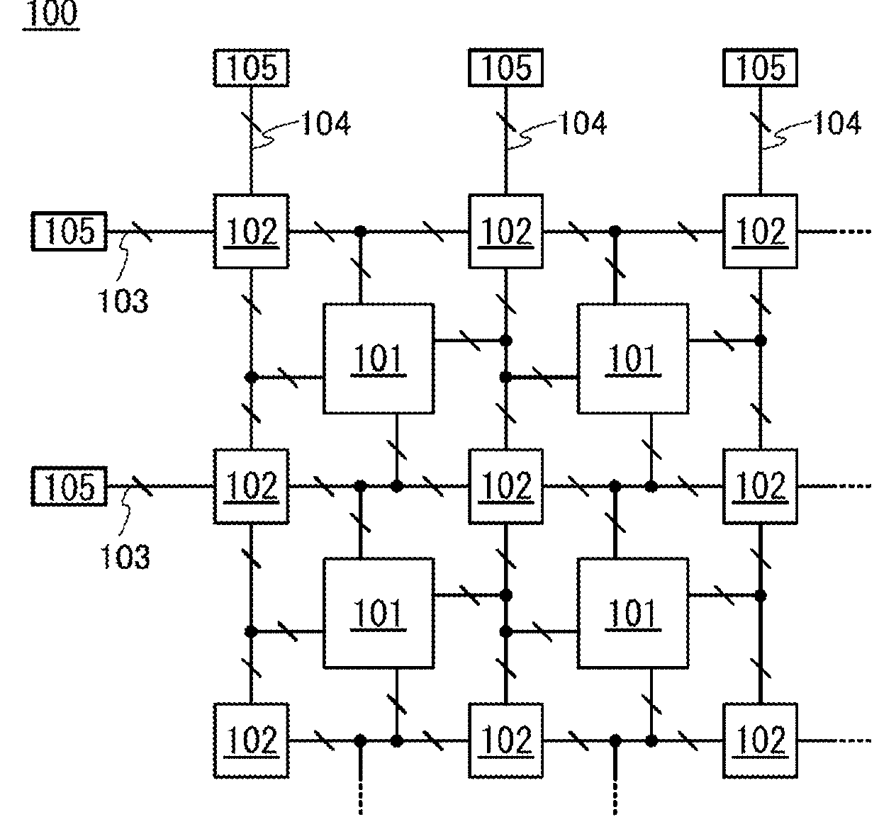
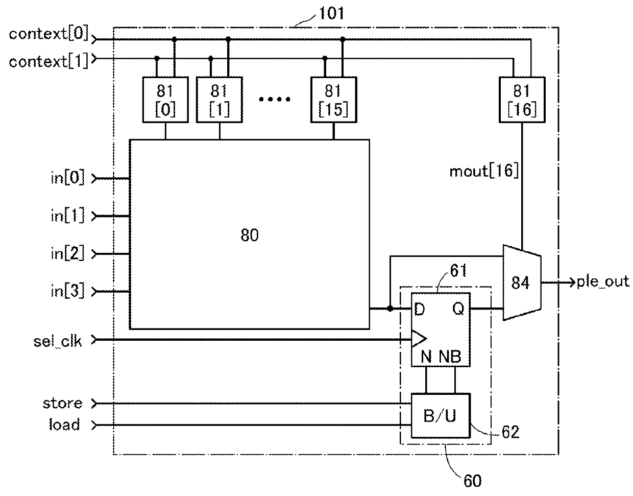
a technology of semiconductor layer and semiconductor layer, applied in the direction of power consumption reduction, pulse technique, instruments, etc., can solve the problems of easy leakage of accumulated charge, difficult to ensure a long data retention time, and increase the current flowing between the gate and the semiconductor layer, so as to reduce power consumption and ensure long data retention time , the effect of short context switch tim

Inactive Publication Date: 2018-06-12
SEMICON ENERGY LAB CO LTD
View PDF19 Cites 0 Cited by
  • Summary
  • Abstract
  • Description
  • Claims
  • Application Information

AI Technical Summary

Benefits of technology

[0010]To achieve lower power consumption, faster operation, or higher integration of a semiconductor device, a semiconductor element such as a transistor used in the semiconductor device needs to be reduced in size. As the size of transistors is reduced, the thickness of a gate insulating film is also reduced according to the scaling law. With a thinner gate insulating film, tunneling current occurs and thus leakage current flowing between a gate and a semiconductor layer increases.
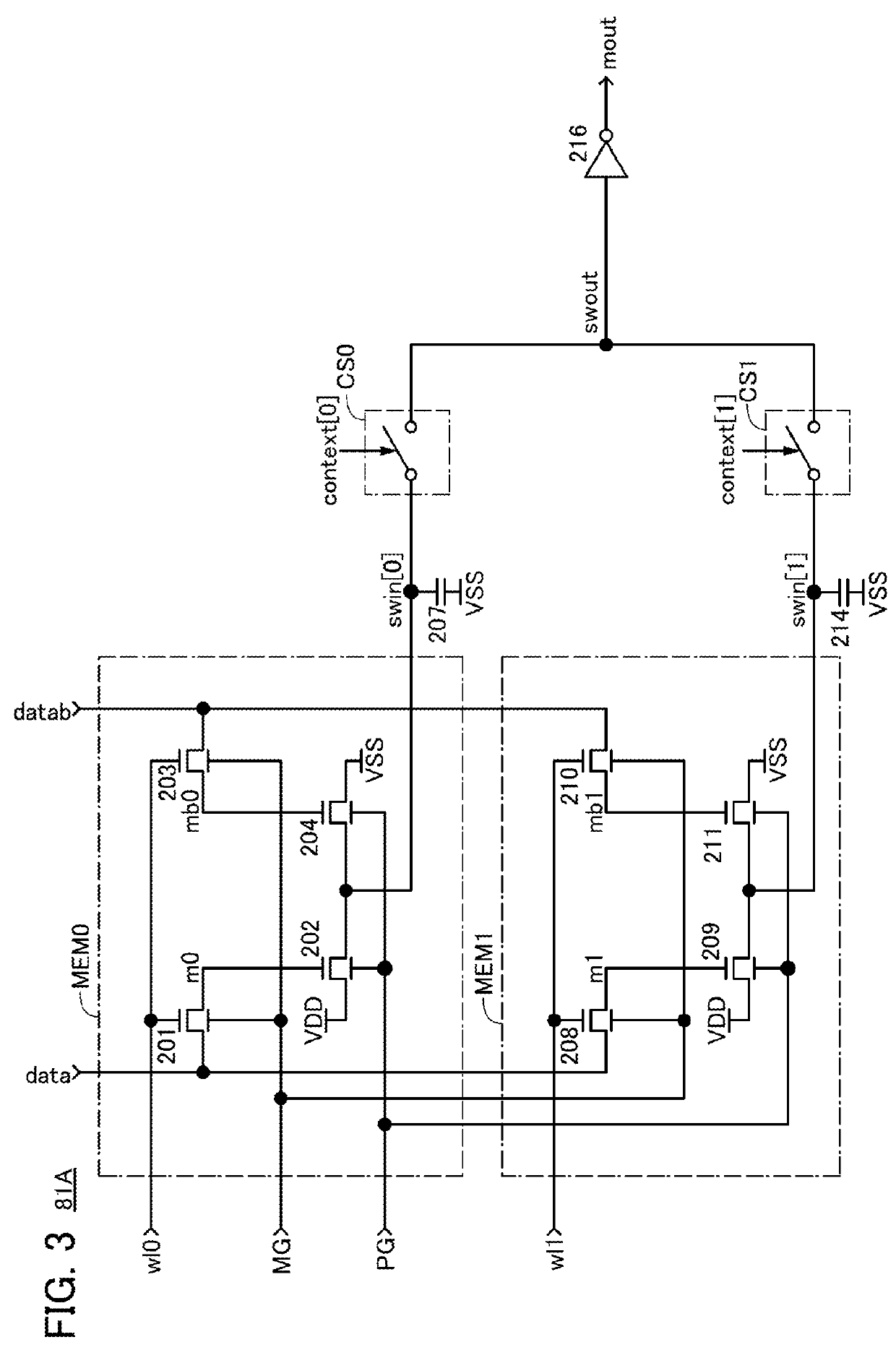
[0011]The semiconductor device in Patent Document 1 (e.g., in FIG. 5B) retains data by accumulating charge at a node between the OS transistor and the Si transistor. In such a semiconductor device, when leakage current of the Si transistor increases because of reduction in size of the semiconductor device, the accumulated charge easily leaks and it becomes difficult to ensure a long data retention time.
[0013]An object of one embodiment of the present invention is to provide a semiconductor device that allows a long data retention time. Another object of one embodiment of the present invention is to provide a semiconductor device that allows reduction in power consumption. Another object of one embodiment of the present invention is to provide a semiconductor device that allows a short context switch time while normal operation is ensured.
[0020]According to one embodiment of the present invention, a semiconductor device that allows a long data retention time can be provided. According to one embodiment of the present invention, a semiconductor device that allows reduction in power consumption can be provided. According to one embodiment of the present invention, a semiconductor device that allows a short context switch time while normal operation is ensured can be provided.

Problems solved by technology

With a thinner gate insulating film, tunneling current occurs and thus leakage current flowing between a gate and a semiconductor layer increases.
In such a semiconductor device, when leakage current of the Si transistor increases because of reduction in size of the semiconductor device, the accumulated charge easily leaks and it becomes difficult to ensure a long data retention time.

Method used


Image

  • Semiconductor device, electronic component, and electronic device
  • Semiconductor device, electronic component, and electronic device
  • Semiconductor device, electronic component, and electronic device

Examples


example 1

[0303]An SRAM-based FPGA in which SRAMs are used for a configuration memory and a register has a difficulty in adopting intermittent operation and normally-off (NOFF) computing which is effective in low-power operation. A nonvolatile FPGA in which nonvolatile memories are used for a configuration memory and a register is proposed.

[0304]For example, Non-Patent Document 2 discloses an MRAM-based FPGA, and Non-Patent Document 3 discloses an FeRAM-based FPGA.

[0305]As described above, a memory formed using an OS transistor with an extremely small off-state current (hereinafter such a memory is referred to as an OS memory) is a nonvolatile memory owing to the extremely small off-state current of the OS transistor. Non-Patent Document 4 discloses NOFF computing with an OS memory-based FPGA (OS FPGA).

[0306]In this example, an OS FPGA is fabricated using a Si-OS hybrid process, and evaluation results of the OS FPGA are reported. The fabricated OS FPGA is referred to as OS FPGA 110. In this e...


PUM


Abstract

Provided is a semiconductor device in which leakage current due to miniaturization of a semiconductor element is reduced and delay at a time of context switch of a multi-context PLD is reduced. A first transistor and a second transistor included in a charge retention circuit functioning as a configuration memory each include an oxide semiconductor in a semiconductor layer serving as a channel formation region. One of a source and a drain of the first transistor is electrically connected to a gate of the second transistor. One of a source and a drain of the second transistor is connected to a switch for context switch. In the switch used for context switch, electrostatic capacitance on an input side to which the one of the source and the drain of the second transistor is connected is larger than electrostatic capacitance on an output side.

Description

BACKGROUND OF THE INVENTION1. Field of the Invention[0001]One embodiment of the present invention relates to a semiconductor device, an electronic component, and an electronic device.2. Description of the Related Art[0002]A programmable logic device (PLD) includes a plurality of programmable logic elements (PLEs) and a plurality of programmable routing switches (PRS's). In the PLD, data on the function of each PLE and data on connection between the PLEs by PRS's are stored as configuration data in a configuration memory. In other words, the PLD stores its circuit structure as configuration data.[0003]A multi-context reconfigurable device is suggested (e.g., Non-Patent Document 1). In the multi-context reconfigurable device, the circuit structure of the PLD is changed by storing a plurality of sets of configuration data corresponding to circuit structures in the PLD and changing configuration data to be used. Configuration data representing a circuit structure is referred to as conte...

Claims


Application Information

Patent Timeline
Patent Type & Authority Patents(United States)
IPC IPC(8): H01L29/78H01L29/786H03K19/00G11C19/28H03K19/177H01L27/12
CPCH03K19/0013G11C19/28H01L27/124H01L27/1207H03K19/1778H01L27/1255H01L29/7851H01L29/7869H01L27/1225
Inventor HARADA, SHINTAROKOZUMA, MUNEHIROKUROKAWA, YOSHIYUKI
Owner SEMICON ENERGY LAB CO LTD
Learn More