
Synchronous semiconductor memory device having an auto-precharge function

Inactive Publication Date: 2000-01-25
SAMSUNG ELECTRONICS CO LTD
View PDF27 Cites 16 Cited by
  • Summary
  • Abstract
  • Description
  • Claims
  • Application Information

AI Technical Summary

Benefits of technology

It is another object of the present invention to provide the synchronous semiconductor memory device having a reliable row chain precharge function.

Problems solved by technology

In a synchronous semiconductor memory device which operates with an external system clock and performs the read / write operation in accordance with the determined burst length and latency information, if the precharge operation of the row chain is performed in response to the precharge command applied from the exterior, as described above, undesirably forcibly determines the proper point in time for precharging the row chain and it is therefore difficult to realize an effective (i.e. reduction of the power consumption) precharge operation.

Method used


Image

  • Synchronous semiconductor memory device having an auto-precharge function
  • Synchronous semiconductor memory device having an auto-precharge function
  • Synchronous semiconductor memory device having an auto-precharge function

Examples


Embodiment Construction

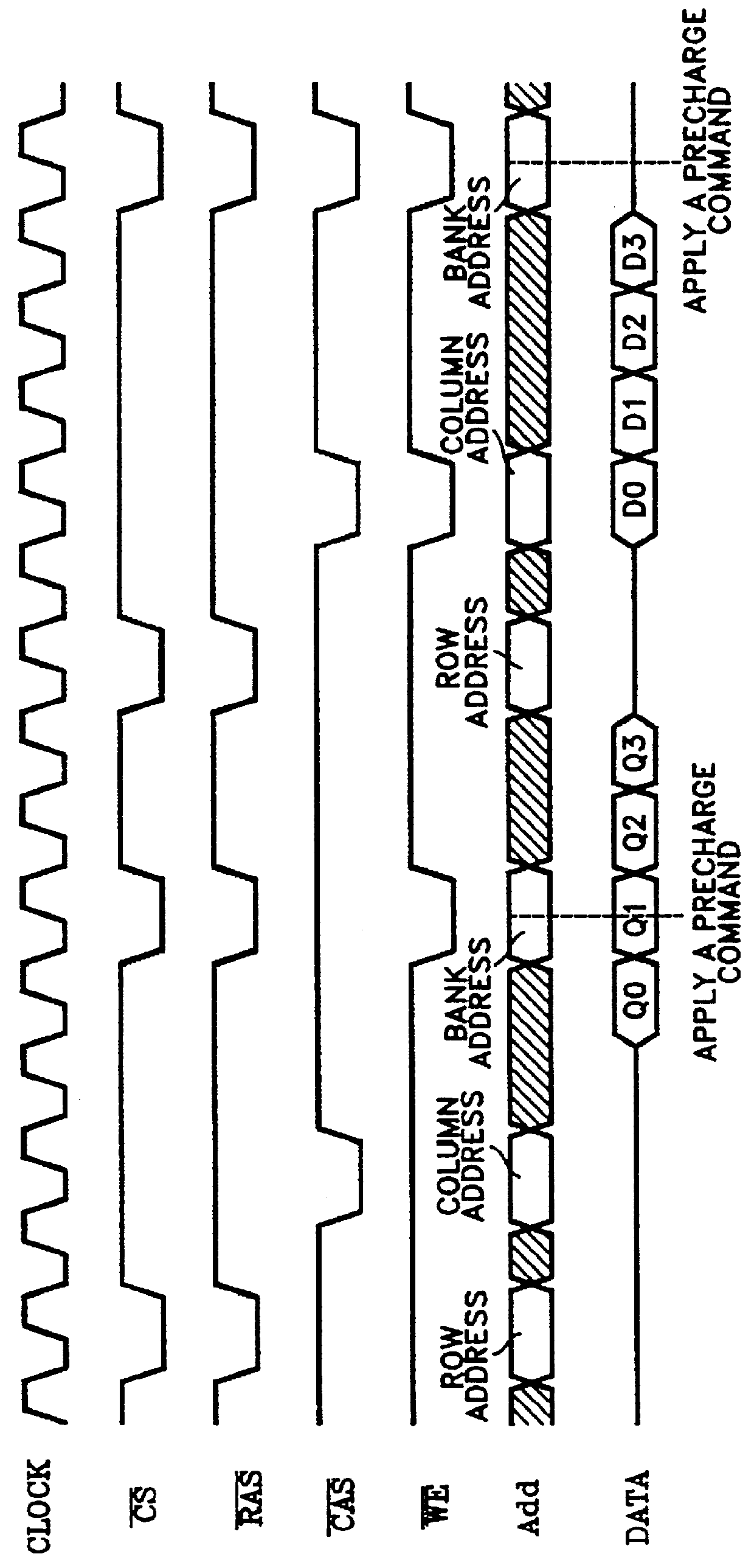
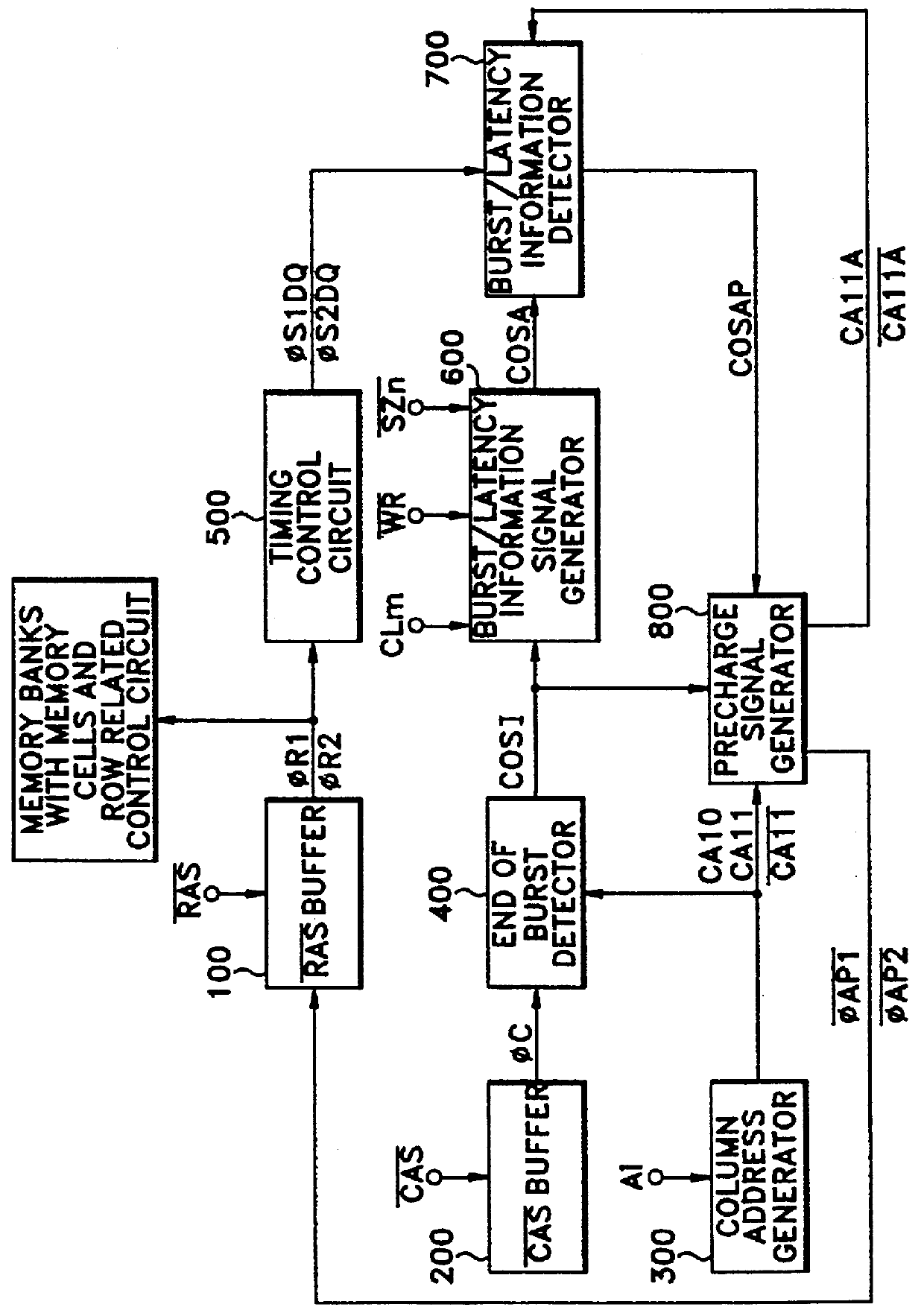
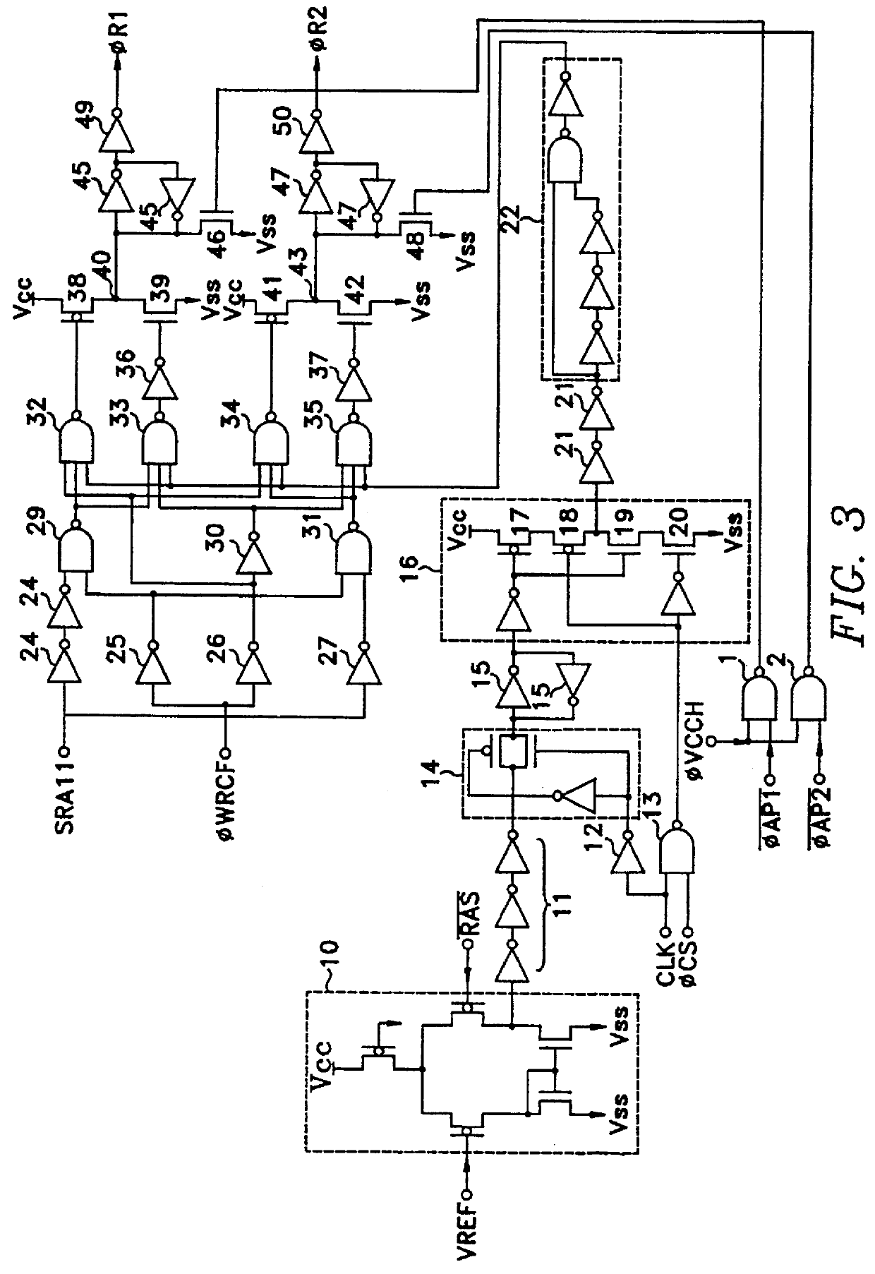
The construction of FIG. 2 required in realizing an auto precharge function according to the present invention includes a RAS buffer 100 that receives a row address strobe signal RAS and then generates row master clocks .phi.R1 and .phi.R2. A CAS buffer 200 receives a column address strobe signal CAS and then generates a column master clock .phi.C which drives column related control circuits. A column address generator 300 receives and buffers an address signal Ai to a CMOS level and then generates a plurality of column address signals (include CA10, CA11 and CA11) from the buffed address signal. An end of burst detector 400 receives the column master clock .phi.C and the counted column address signals and then generates a burst length detection signal COSI which detects the end state of the burst length. A timing controller 500 receives the row master clocks .phi.R1 and .phi.R2 and then generates timing control signals .phi.S1DQ and .phi.S2DQ. A burst / latency information signal gen...


PUM


Abstract

A semiconductor memory device according to the present invention having a plurality of memory banks, a row address strobe signal buffer, a column address strobe signal buffer and a column address generator and performing a data access operation in response to the burst length and latency information related to a system clock having a predetermined frequency, comprises a device for generating a signal which automatically precharges one memory bank of the memory banks in response to the row address strobe signal and the signal having the burst length and latency information after an address operation for the memory bank is completed.

Description

BACKGROUND OF THE INVENTIONThe present invention relates to a semiconductor memory device for precharging a row chain, and particularly to a synchronous semiconductor memory device for automatically precharging the row chain.The synchronous semiconductor memory device, which has been developed for high speed operation, performs all operations required in accessing data corresponding to a system clock (or a synchronous clock) of constant period supplied from externally. With the use of a mode set register, such a synchronous semiconductor memory device sets various operation modes for determining the latency and burst length. In semiconductor memory device, if a read or write operation of one row is completed, the activated row chain must be precharged in order to perform the read or write operation of another row.As shown in FIG. 1, in a conventional semiconductor memory device, the row chain is precharged only when a precharge command is applied from the exterior of the device afte...

Claims


Application Information

Patent Timeline
IPC IPC(8): G11C7/00G11C7/12G11C7/10
CPCG11C7/1072G11C7/12
Inventor KIM, GYU-HONG
Owner SAMSUNG ELECTRONICS CO LTD
Features
  • Generate Ideas
  • Intellectual Property
  • Life Sciences
  • Materials
  • Tech Scout
  • Unparalleled Data Quality
  • Higher Quality Content
  • 60% Fewer Hallucinations
Learn More