Wafer polishing method and apparatus

Inactive Publication Date: 2002-04-02
NOVELLUS SYSTEMS
View PDF26 Cites 11 Cited by
  • Summary
  • Abstract
  • Description
  • Claims
  • Application Information

AI Technical Summary

Benefits of technology

Wafer polishing apparatus in accordance with the present invention comprises a polishing assembly having a plurality of wafer carriers for substantially simultaneously engaging a plurality of wafers of material with a polishing surface. The apparatus includes an index table for holding wafers to be polished, and positioning apparatus to move the polishing assembly between the polishing surface and the index table. At the index

Problems solved by technology

Each wafer is of relatively high cost due to

Method used


Image

  • Wafer polishing method and apparatus
  • Wafer polishing method and apparatus
  • Wafer polishing method and apparatus

Examples


Embodiment Construction

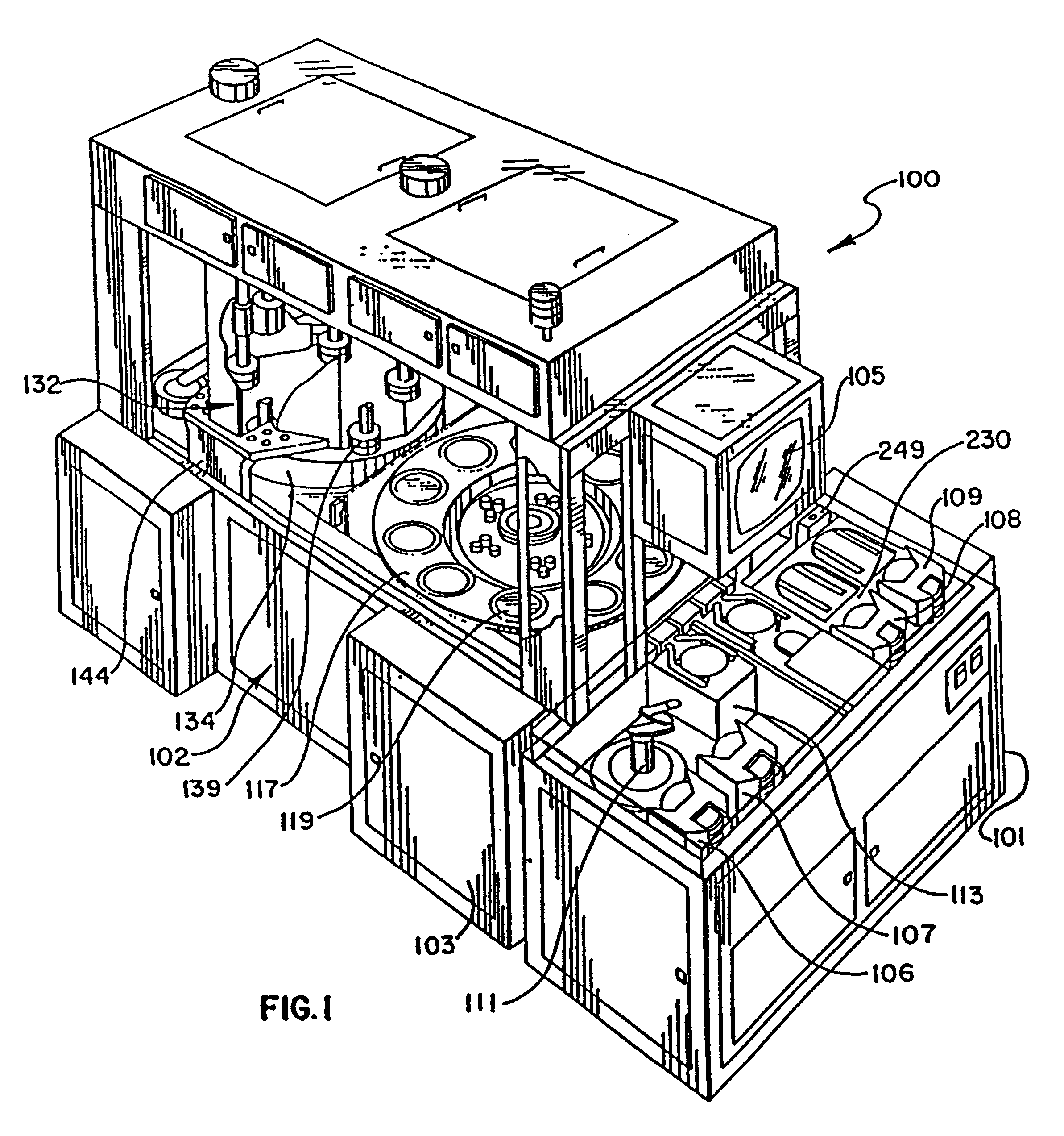
FIG. 1 is a perspective view of a wafer polishing apparatus 100 embodying the present invention. Wafer polishing apparatus 160 includes a wafer input / output module 101 and a wafer process module 102. The wafer polishing apparatus 100 is constructed so that input / output module 101 can be placed, for example, inside a class 10 clean room environment while the process module 102 is placed beyond an adjacent wall perhaps in a class 1000 clean room environment. By means not specifically shown, air flow is created within the polishing system and the air pressures are regulated such that the environment of the class 10 clean room is not negatively influenced.

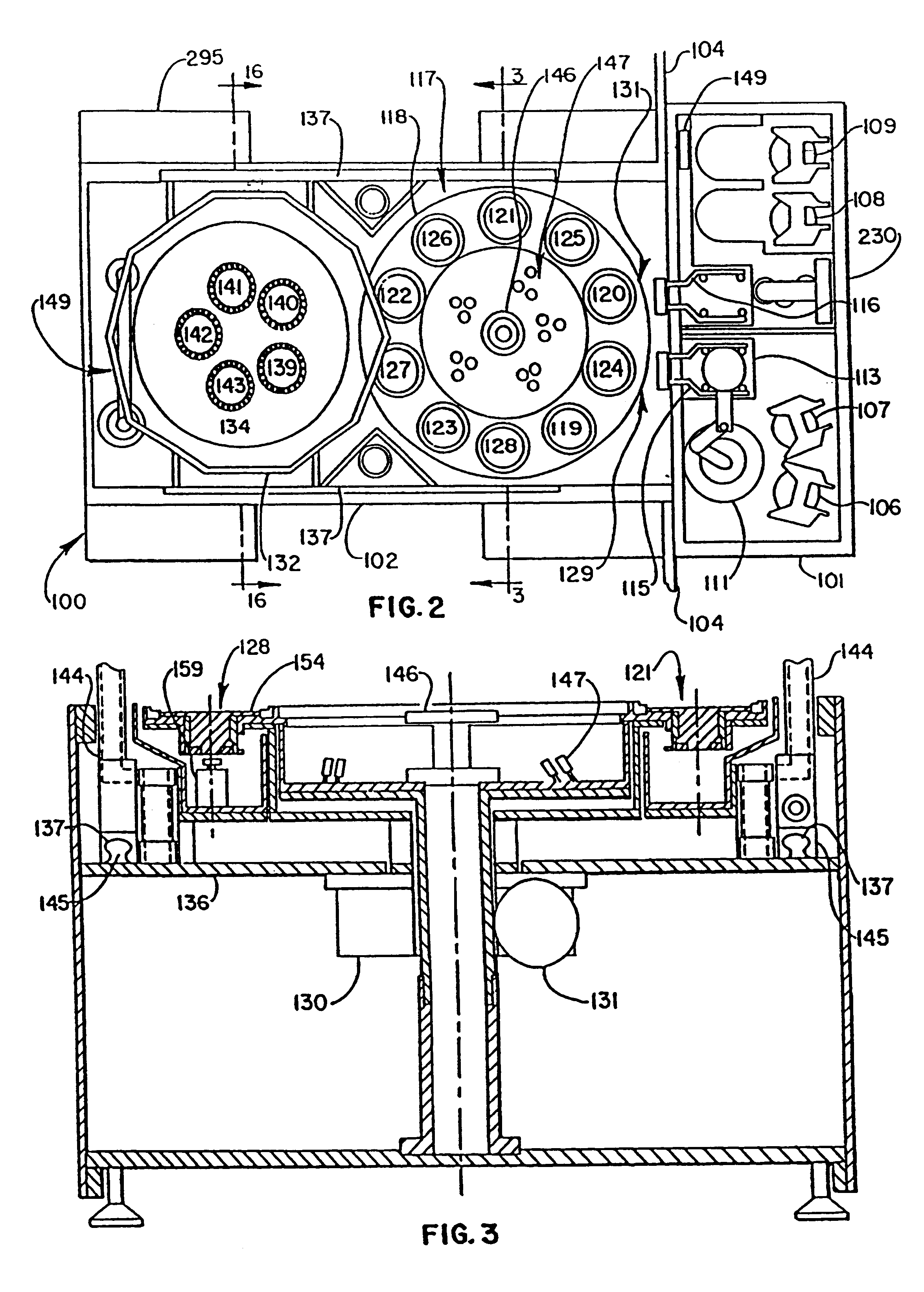
FIG. 2 is a top view of wafer polishing apparatus 100 in which the top and certain other structure of the perspective view has been removed for ease of understanding. Additionally in FIG. 2, a wall 104 is represented showing separation of input / output module 101 and process module 102 thereby. Wafers are presented to and removed from i...


PUM


Abstract

A wafer polishing apparatus includes a wafer polishing assembly having a plurality of wafer carriers for substantially simultaneously polishing a plurality of wafers against a rotating polishing surface. A plurality of wafers to be polished are substantially simultaneously loaded into the plurality of wafer carriers by wafer holding apparatus of an index table. Similarly, a plurality of wafer carriers are substantially simultaneously unloaded into wafer holding apparatus of the index table. The wafer carriers are individually computer controlled for exact polishing and different polishing requirements can be met at the same time by different wafer carriers.

Description

BACKGROUND OF THE INVENTIONThis invention relates to polishing methods and apparatus and more particularly, to such methods and apparatus for accurately polishing wafers of semiconductor material with high throughput and in a manner compatible with semiconductor processing clean room environments.The production of integrated circuits begins with the creation of high quality semiconductor wafers. Each wafer is of relatively high cost due to the detailed processing needed to produce it. During the integrated circuit production process, an extremely flat surface is desired on at least one face of the wafer. Wafer polishing to achieve such a flat surface is a known technique.Such polishing generally includes attaching one side of the wafer to a flat surface of a wafer carrier or chuck and pressing the wafer against a flat polishing surface. The polishing surface is moved under the wafer, and the wafer may also be rotated about its vertical axis and oscillated back and forth to improve p...

Claims


Application Information

Patent Timeline
IPC IPC(8): B24B49/16B24B37/04B24B51/00G05B19/418H01L21/67H01L21/677H01L21/683B24B37/08B24B37/34H01L21/304
CPCB24B37/08H01L21/6838B24B49/16B24B51/00G05B19/41825H01L21/67745H01L21/67751B24B37/345G05B2219/37399G05B2219/45026G05B2219/45199G05B2219/45232G05B2219/49356G05B2219/49361G05B2219/50007G05B2219/50362G05B2219/50371G05B2219/50381G05B2219/50388Y02P90/02B24B37/04H01L21/304
Inventor KARLSRUD, CHRIS E.VAN WOERKOM, ANTHONY G.ODAGIRI, SHIGERUNAGAHASHI, ISAO
Owner NOVELLUS SYSTEMS
Why Eureka
Try Eureka