
Method of and apparatus for providing look ahead column redundancy access within a memory

Inactive Publication Date: 2009-11-24
FOOTHILLS IP LLC +1
View PDF13 Cites 0 Cited by
  • Summary
  • Abstract
  • Description
  • Claims
  • Application Information

AI Technical Summary

Benefits of technology

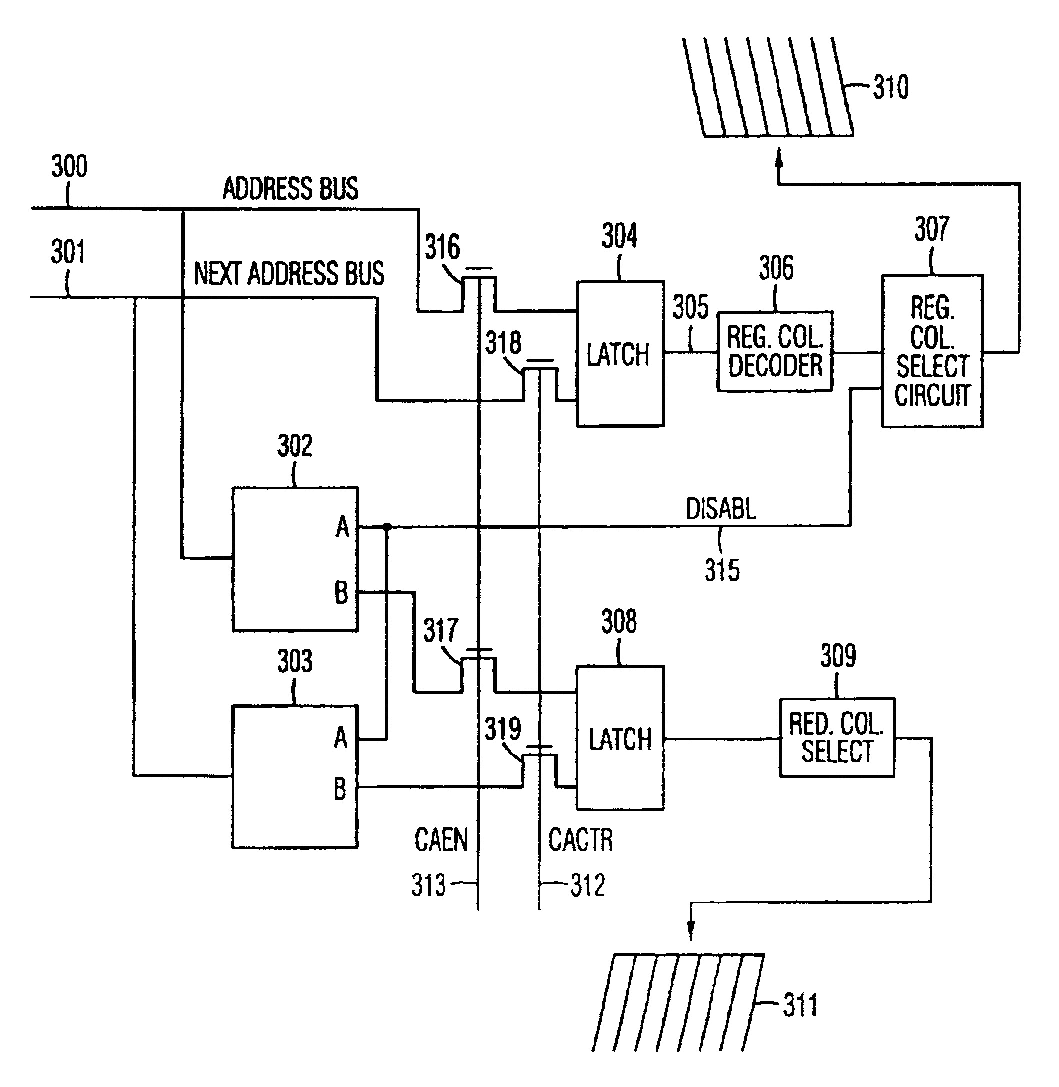
[0014]A look ahead column redundancy circuit provides high speed memory access to both regular memory arrays and redundant memory arrays. In the preferred embodiment of the present invention, the information on both the address bus and the information on the next address bus are decoded by redundant column decoders in parallel. The decoded information from the redundant column decoders is then provided to a redundancy column pathway as the addressing information from the address bus and the next address bus is provided to a main column pathway through a latch. The information on the address bus is latched when beginning at a new column address. The information on the next address bus is latched for the next column address when operating in a burst cycle mode. The main column pathway preferably includes a main column decoder and a main column select circuit. A disable signal is also activated by the redundant column decoders if the addressing information for a current memory access operation corresponds to an address within the redundant memory array. When activated, the disable signal disables the main column select circuit within the main column pathway. If the addressing information for a current memory access operation does not correspond to an address within the redundant memory array, then the memory access operation is performed within the main memory array within any additional delays. Since the decoding is performed before the information is latched onto the column address bus, the proper pathway is selected without the need for any additional delay.
[0015]In one aspect of the present invention, an apparatus for accessing a memory structure including a main memory array and a redundant memory array comprises an address bus for carrying addressing information for a current memory access operation, a main column pathway including a main column decoder for decoding addressing information and a main select circuit for selecting appropriate groups of memory cells within the main memory array for a current memory access operation and a redundant column pathway including a redundant column decoder for decoding addressing information and a redundant select circuit for selecting appropriate groups of memory cells within the redundant memory array for a current memory access operation if the current memory access operation is accessing memory cells within the redundant memory array, wherein the redundant column pathway is selected if the current memory access operation is accessing memory cells within the redundant memory array. The redundant column decoder disables the main select circuit if the current memory access operation is accessing memory cells within the redundant memory array. The redundant column decoder is provided the addressing information before the main column pathway. The main column pathway is provided the addressing information and the redundant select circuit is provided decoded redundant addressing information from the redundant column decoder in response to a control signal. The groups of memory cells are columns.
[0016]In another aspect of the present invention, a method of completing memory access operations within a memory structure including a main memory array and a redundant memory array, comprises the steps of determining from addressing information for a current memory access operation if the addressing information represents an address included within the redundant memory array, decoding a redundant address within the redundant memory array, if the addressing information represents an address included within the redundant memory array, providing the addressing information for the current memory access operation to a main column pathway and providing the redundant address to a redundant column pathway in response to a first control signal, decoding a main address within the main memory array corresponding to the addressing information; activating a group of main memory cells within the main memory array corresponding to the main address and selecting the redundant column pathway if the addressing information represents an address included within the redundant memory array. The method further includes the step of disabling the step of activating

Problems solved by technology

In general, as integration density in semiconductor memory devices increases, the likelihood of defective cells in any one memory array also increases.
Therefore, the higher the integration density of chips fabricated on a given wafer, the lower the wafer yield.
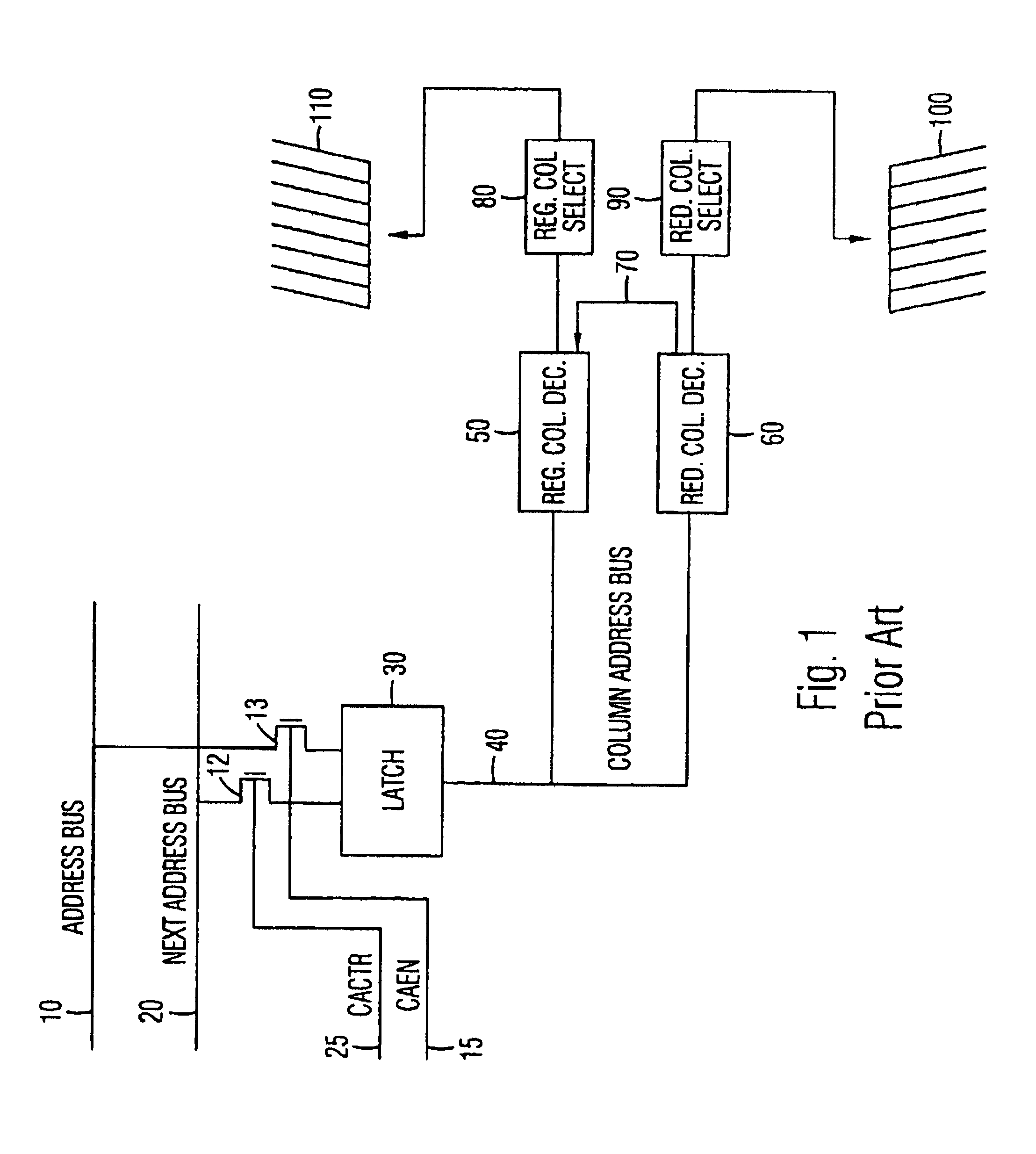
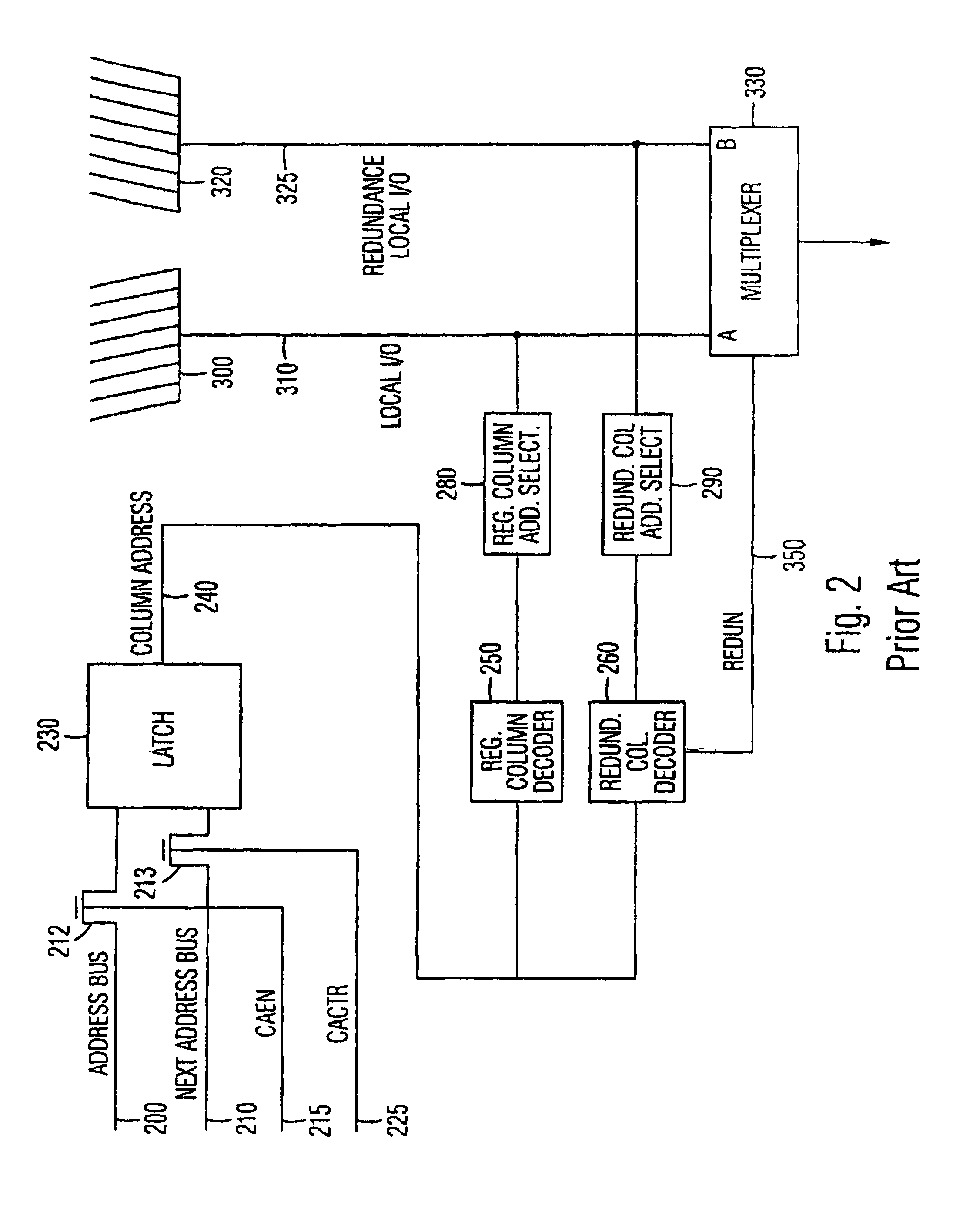
One problem which exists with the use of redundant memory circuits as substitutes for main memory circuits is access time.
This waiting causes delays and extends the time necessary for each memory access operation.
This solution will speed up access time during memory access operations but requires significant additional layout at the cost of additional space and complexity.

Method used


Image

  • Method of and apparatus for providing look ahead column redundancy access within a memory
  • Method of and apparatus for providing look ahead column redundancy access within a memory
  • Method of and apparatus for providing look ahead column redundancy access within a memory

Examples


Embodiment Construction

[0021]A look-ahead column redundancy circuit of the present invention includes a main memory pathway and a redundancy pathway in order to minimize memory access time and delays during memory access operations. Addressing information from an address bus and a next address bus is provided to a pair of redundant column decoders. The redundant column decoders decode the addressing information and determine if the addressing information corresponds to an address within the redundant memory array. The decoded information from the redundant column decoders is then provided to a redundancy column pathway as the addressing information from the address bus and the next address bus is provided to a main column pathway. The main column pathway includes a latching circuit, a main column decoder and a main column select circuit. A disabling signal is activated by the redundant column decoders if the addressing information for the current memory access operation corresponds to an address within th...


PUM


Abstract

A look ahead column redundancy circuit provides high speed memory access to both regular memory arrays and redundant memory arrays. In the preferred embodiment of the present invention, the information on both the address bus and the information on the next address bus are decoded by redundant column decoders in parallel. The decoded information from the redundant column decoders is then provided to a redundancy column pathway as the addressing information from the address bus and the next address bus is provided to a main column pathway. The information on the address bus is latched when beginning at a new column address. The information on the next address bus is latched for the next column address when operating in a burst cycle mode. The main column pathway preferably includes a latch, a main column decoder and a main column select circuit. A disable signal is also activated by the redundant column decoders if the addressing information for a current memory access operation corresponds to an address within the redundant memory array. When activated, the disable signal disables the main column select circuit within the main column pathway. If the addressing information for a current memory access operation does not correspond to an address within the redundant memory array, then the memory access operation is performed within the main memory array without any delays. Since the decoding is performed before the information is latched onto the column address bus, the proper pathway is selected without the need for any additional delay.

Description

RELATED APPLICATIONS:[0001]This application claims priority under 35 U.S.C. §119(e) of the co-pending U.S. provisional application Ser. No. 60 / 128,039 filed on Apr. 6, 1999 and entitled “METHOD OF AND APPARATUS FOR PROVIDING LOOK AHEAD COLUMN REDUNDANCY ACCESS WITHIN A MEMORY.” The provisional application Ser. No. 60 / 128,039 filed on Apr. 6, 1999 and entitled “METHOD OF AND APPARATUS FOR PROVIDING LOOK AHEAD COLUMN REDUNDANCY ACCESS WITHIN A MEMORY” is also hereby incorporated by reference.FIELD OF THE INVENTION[0002]The present invention generally relates to semiconductor memory devices. More particularly, the present invention relates to redundancy circuits within semiconductor memory devices.BACKGROUND OF THE INVENTION[0003]Random access memory (RAM) is a component used within electronic systems to store data for use by other components within the system. Dynamic RAM (DRAM) is a type of RAM which uses a capacitor-type storage and requires periodic refreshing in order to maintain ...

Claims


Application Information

Patent Timeline
IPC IPC(8): G06F11/00G11C11/401G06F12/16G11C11/408G11C29/00G11C29/04
CPCG11C29/842
Inventor TSAI, TERRY T.MCLAUGHLIN, DANIEL F.
Owner FOOTHILLS IP LLC
Learn More