Semiconductor device and its lead frame
A semiconductor and lead technology, applied in the direction of semiconductor devices, circuit devices, semiconductor/solid-state device components, etc., can solve the problem of not being able to reduce the installation area of semiconductor devices
- Summary
- Abstract
- Description
- Claims
- Application Information
AI Technical Summary
Problems solved by technology
Method used
Image
Examples
Embodiment 1
[0060] Hereinafter, Embodiment 1 will be described with reference to the drawings.
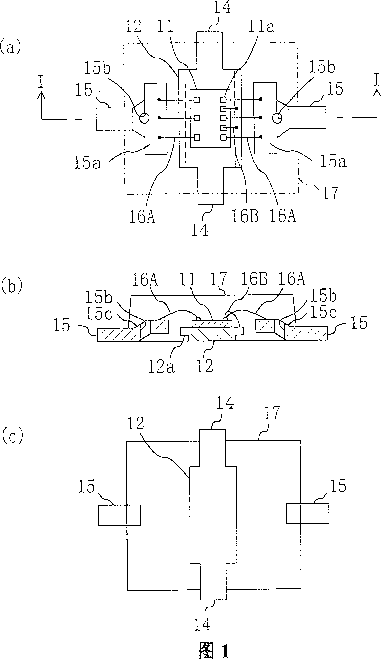
[0061] FIG. 1 is a semiconductor device according to Embodiment 1 of the present invention. Wherein, Fig. 1 (a) shows the structure front view of semiconductor device; Fig. 1 (b) shows the I-I line structure sectional view of Fig. 1 (a); Fig. 1 (c) shows that this semiconductor device is installed on the side such as substrate bottom view of the structure. As shown in Figure 1 (a), this semiconductor device has a semiconductor chip 11 forming a semiconductor element of a high-frequency integrated circuit, a square chip base 12 mounted on the semiconductor chip 11, and each inner end portion is aligned with the short side of the chip base 12. The first leads 14 formed by connecting the side ends, and a pair of second leads 15 respectively extending outside each end sandwich the chip base with intervals. Here, the mounting surface of the semiconductor chip 11 of the die pad 12 is formed by sel...
Embodiment 2
[0084] Hereinafter, Embodiment 2 of the present invention will be described with reference to the accompanying drawings.
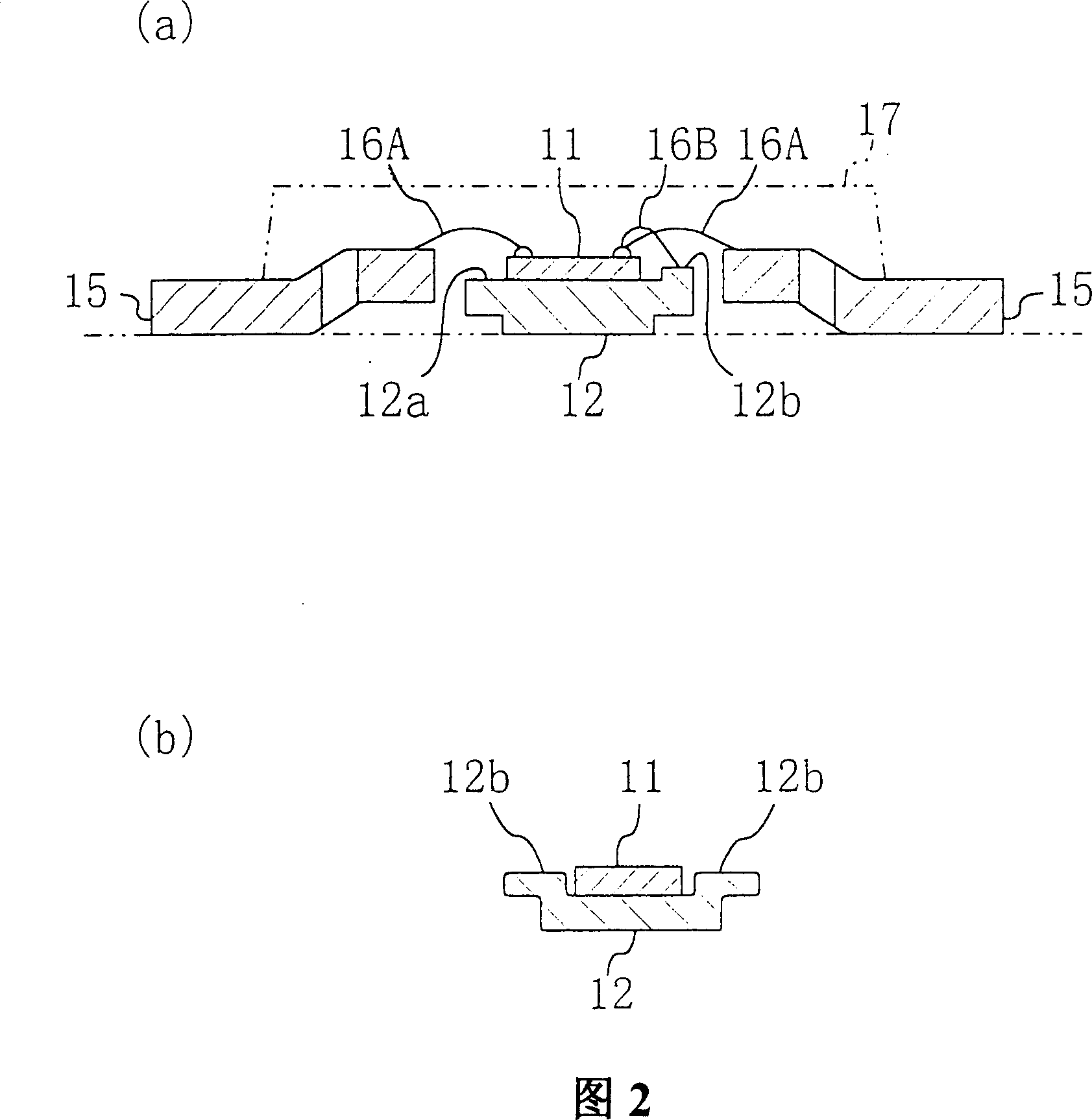
[0085] FIG. 2 shows the structure of a semiconductor device according to Embodiment 2 of the present invention. Wherein, FIG. 2(a) shows the cross-sectional structure of the semiconductor device; FIG. 2(b) only shows the cross-sectional structure of the chip base. FIG. 2( a ) shows the same cross-sectional structure as in FIG. 1( b ), which is connected to a first lead (not shown) and perpendicular to the extending direction of the first lead. In FIG. 2( a ), the same components as those shown in FIG. 1( b ) are denoted by the same reference numerals, and description thereof will be omitted. Thin-layer portions 12a are respectively provided on both sides of the mounting surface of the chip base 12 in this embodiment, and at the same time, on the other thin-layer portion, a thickness of 5% to 100% of the thickness of the semiconductor chip 11 is provided a...
Embodiment 3
[0092] Hereinafter, Embodiment 3 of the present invention will be described with reference to the drawings.
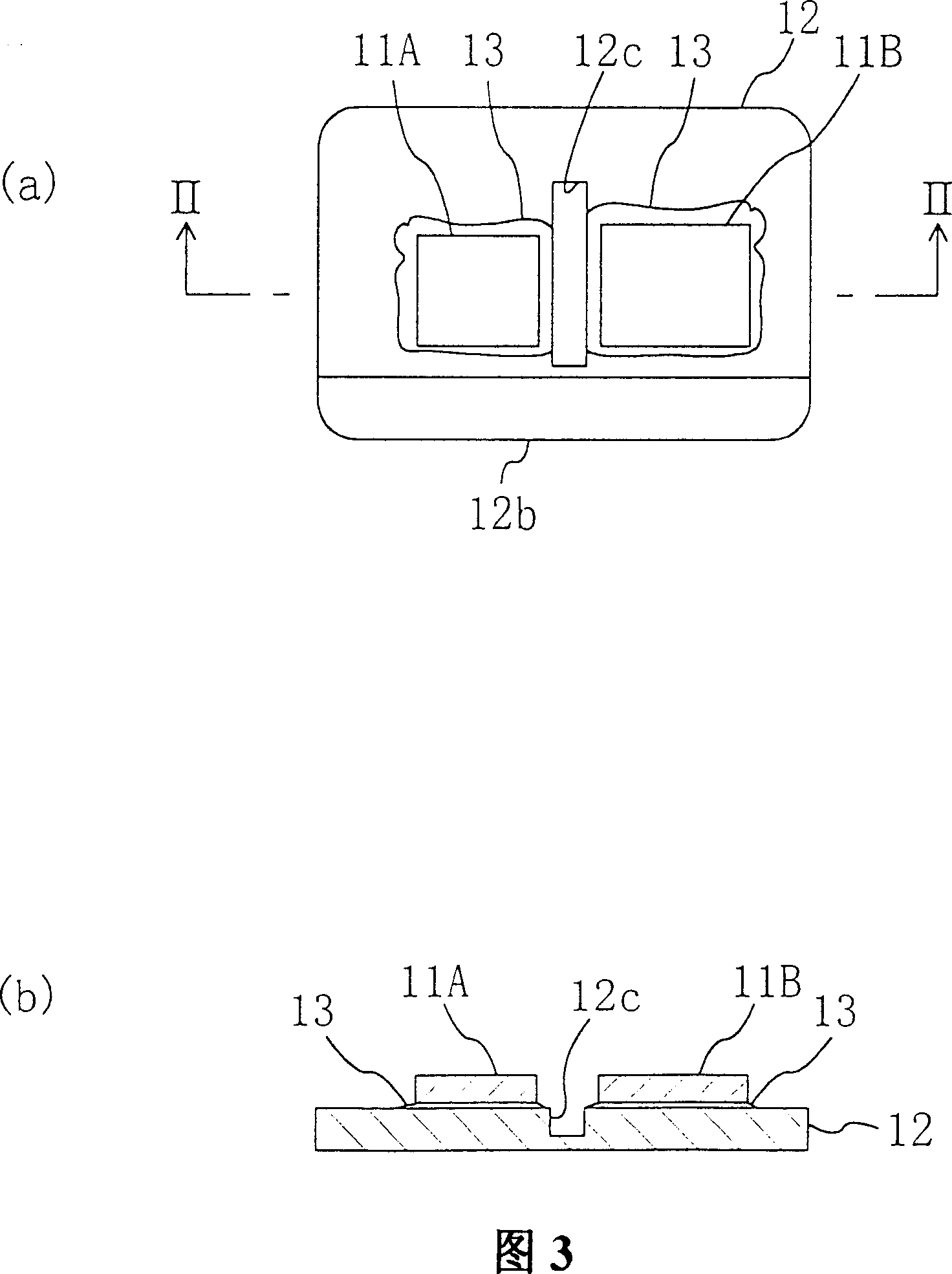
[0093] Fig. 3 shows the structure of the semiconductor device of embodiment 3 of the present invention, wherein Fig. 3 (a) shows the plane structure of the chip base in this semiconductor device; Fig. 3 (b) shows II-II of Fig. 3 (a) The cross-sectional structure of the line. In FIGS. 3( a ) and ( b ), the same components as those shown in FIG. 2( a ) are denoted by the same reference numerals, and description thereof will be omitted. As shown in FIG. 3( a), on the mounting surface of the chip base 12, an inner square shape is formed at the center thereof, extending in a vertical direction to the long side of the chip base 12, and simultaneously forming a concave portion on the mounting surface to prevent the diffusion of the fixing material 12c. ; The first semiconductor chip 11A and the second semiconductor chip 11B are respectively fixed on the chip base with the fi...
PUM
 Abstract
Description
Claims
Application Information
 - R&D
- Intellectual Property
- Life Sciences
- Materials
- Tech Scout
- Unparalleled Data Quality
- Higher Quality Content
- 60% Fewer Hallucinations
Browse by: Latest US Patents, China's latest patents, Technical Efficacy Thesaurus, Application Domain, Technology Topic, Popular Technical Reports.
© 2025 PatSnap. All rights reserved.Legal|Privacy policy|Modern Slavery Act Transparency Statement|Sitemap|About US| Contact US: help@patsnap.com


