A differential interconnection circuit

A circuit and differential technology, which is applied in the field of capacitance superimposed circuits, can solve the problems such as inability to multiplex differential signals, and achieve the effects of avoiding repeated development, saving costs, and reducing types

Inactive Publication Date: 2008-01-02
ZTE CORP
View PDF0 Cites 0 Cited by
  • Summary
  • Abstract
  • Description
  • Claims
  • Application Information

AI Technical Summary

Problems solved by technology

[0004] The purpose of the present invention is to overcome the shortcoming that the signal bifurcation in the prior art affects the signal integrity, and solve the problem that the differential signal cannot be multiplexed in the prior art

Method used


Image

  • A differential interconnection circuit
  • A differential interconnection circuit
  • A differential interconnection circuit

Examples


example 1

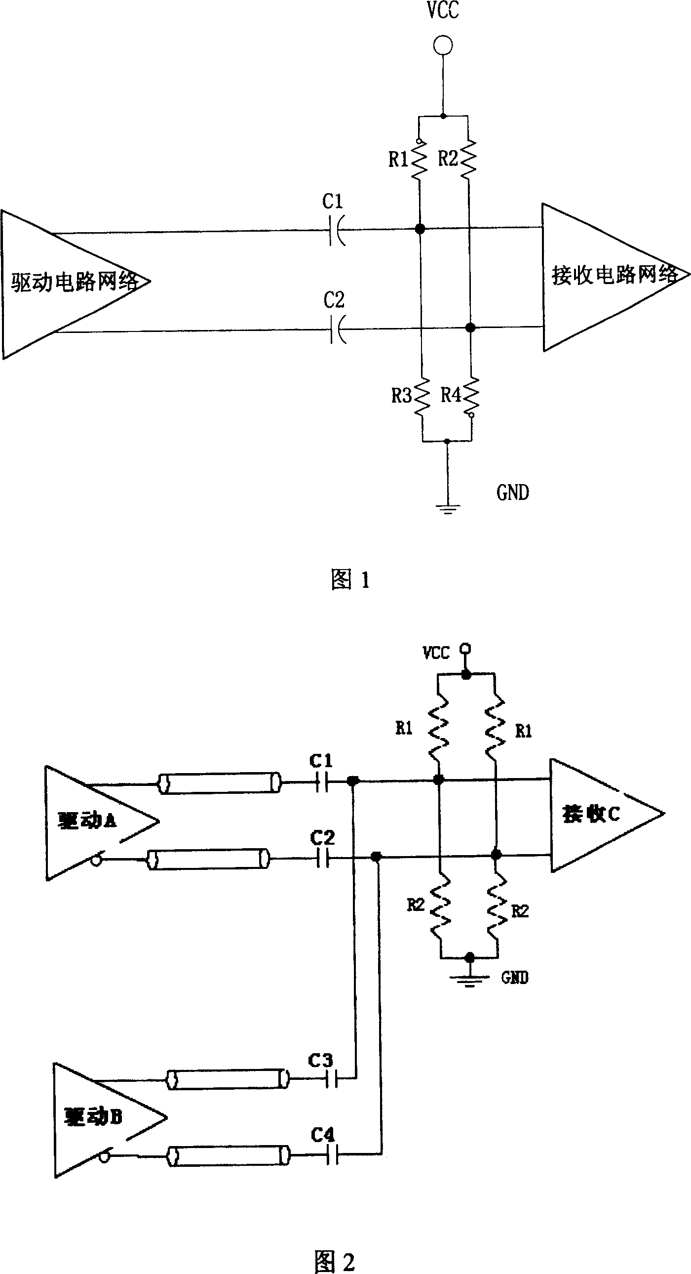
[0024] Example 1: When designing a single board, it is often encountered that it is not sure which one will be used for the final design, because it involves many factors in the supply price and performance of the chip. In this case, it is necessary to design When packaging the two devices, it is generally difficult to achieve pin-level compatibility for chips with more complex functions. In this case, the method of the present invention needs to be used to solve the signal integrity problem. For example, in the example of an SDH optical board, the signal of an optical module is a differential signal of LVPECL level. There are two optional SDH FRAME chips here. At this time, the method proposed by the present invention needs to be used to process the signal. Ensure the integrity of the signal between the optical module and SDH FRAME.

example 2

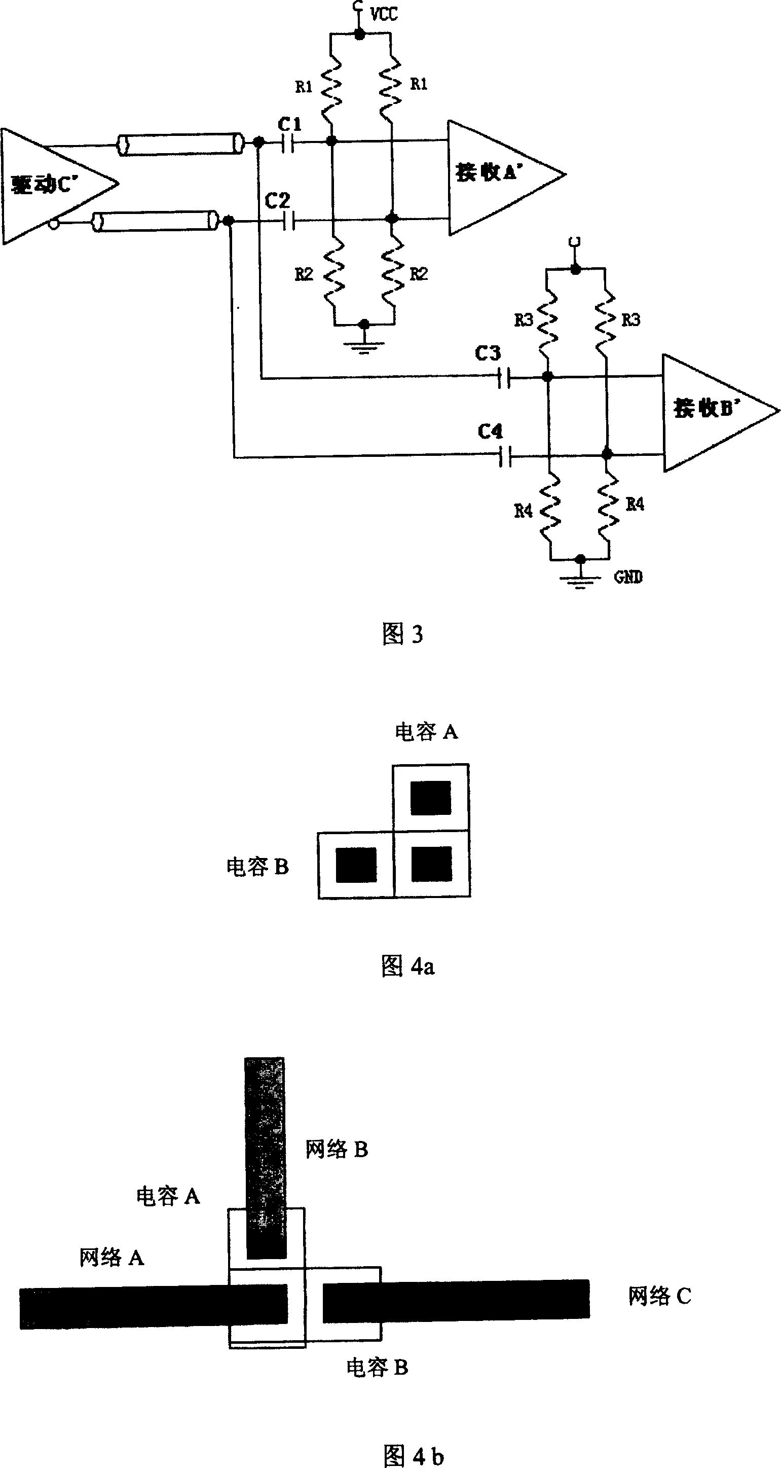
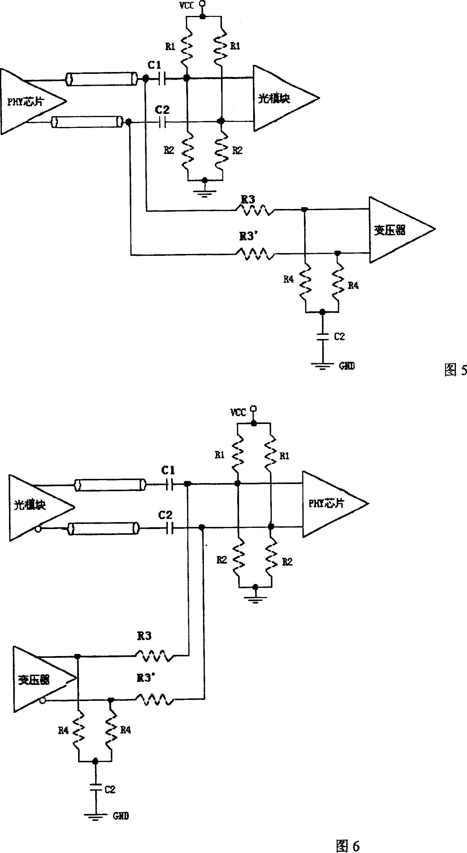
[0025] Example 2: In the actual design, a PHY chip supporting 8 100M ports is used. This PHY chip supports connection with optical ports and electrical ports, but the pins are the same group of pins, which support multiplexing. Through a mode Choose the foot to achieve. See Figure 5 and Figure 6 for specific schematic diagrams.

[0026] In the design, it is hoped that the 100M board can be made into an optical port board or an electrical port board, that is to say, it can support 8 ports that are all 100M optical ports or 8 ports that are all 100M electrical ports.

[0027] However, since the interface of the PHY chip is a differential signal, the bifurcation of the signal line cannot be connected to the 100M optical module and the 100M electrical port transformer. Therefore, it is necessary to implement multiplexing through capacitive connection according to the AC matching described above. In this way, the bifurcation problem of the signal line is avoided, and the integrity...


PUM


Abstract

The invention discloses a difference interconnected circuit, for two-driving and one-receiving condition, which includes: driving circuit networks an and B, receiving circuit network C and AC matched patch capacitors C1, C2, C3 and C4; where network A's output ends are in series with the two capacitors C1 and C2, respectively and the network B's output ends are in series with the two capacitors C3 and C4; the other ends of the capacitors C1 and C2 are overlapped with those of the capacitors C3 and C4 on the pads to form tow output ports, respectively, where the two ports are connected with two input ends of the capacitor C, respectively. It can reduce kinds of single plates in a system and save cost, and support the range from low-frequency and high-frequency without speed limit, and also support conversion between different forms of signals.

Description

technical field [0001] The invention relates to a capacitance superposition circuit for realizing differential signal selection, in particular to the situation that differential pins in the (communication) field are connected to different devices in different application occasions. Background technique [0002] Generally, an electronic system, especially a communication system, is composed of many chips, and there are two ways of interconnection among the chips: direct current and alternating current. The DC method is suitable for the interconnection of the same signal format, while the AC coupling is more applicable to the interconnection of heterogeneous signal formats, and can transform the signal format into a network. The same pin of one chip is connected to different pins of multiple chips at the same time, that is, the so-called one-to-many connection method, which is a very common requirement in the design of communication systems. Due to the low speed, the signal i...

Claims


Application Information

Patent Timeline
Patent Type & Authority Patents(China)
IPC IPC(8): H04B1/04H03H7/00
Inventor 王静璇李明生
Owner ZTE CORP
Why Eureka
Try Eureka