Detecting structure for simultaneously detecting hot carriers of multiple metal-oxide-semiconductor device

A hot carrier and test structure technology, applied in semiconductor/solid-state device testing/measurement, semiconductor devices, electrical components, etc., can solve problems such as gate oxide layer damage and charge accumulation

Inactive Publication Date: 2008-01-16
SEMICON MFG INT (SHANGHAI) CORP +1
View PDF6 Cites 2 Cited by
  • Summary
  • Abstract
  • Description
  • Claims
  • Application Information

AI Technical Summary

Problems solved by technology

In the MOS process manufacturing process, there will be many plasma process steps.

Method used


Image

  • Detecting structure for simultaneously detecting hot carriers of multiple metal-oxide-semiconductor device
  • Detecting structure for simultaneously detecting hot carriers of multiple metal-oxide-semiconductor device

Examples


Embodiment Construction

[0019] Referring to accompanying drawing 1 and accompanying drawing 2 below, describe the present invention in detail.

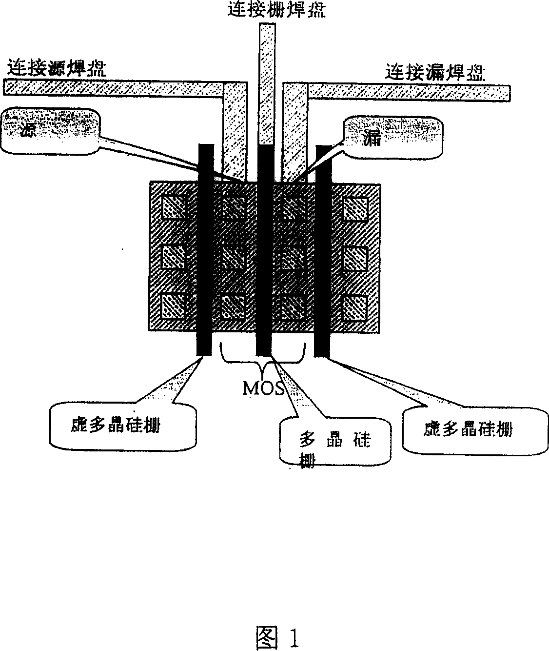
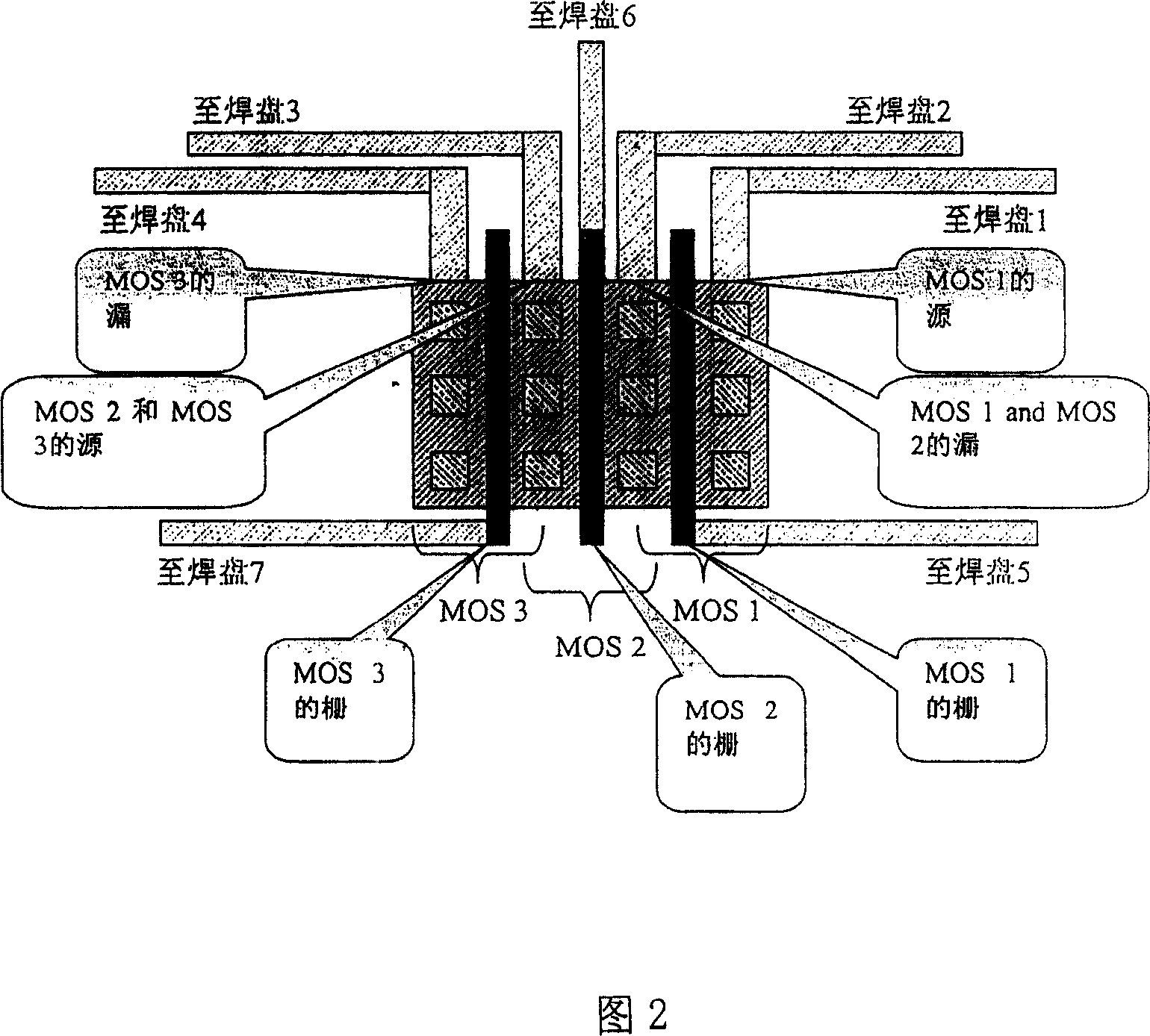
[0020] FIG. 1 is a test structure of an existing MOS device. In the test structure of the MOS device shown in FIG. 1 , there is a polysilicon gate, two sides of the polysilicon gate have a source region and a drain region, and the other side of the source region and the drain region has a drain region and a source region. The polysilicon gate and its side source and drain regions constitute a MOS device unit, and the polysilicon gate and its side source and drain regions are connected to respective pads through metal wires to form a test structure of the MOS device. The dummy polysilicon gate and the area other than the dummy polysilicon gate are not connected to the pad separately, and the dummy polysilicon gate only plays a role in preventing the microscopic effect and etching speed from affecting the length of the polysilicon gate during the etching proce...


PUM


Abstract

The detection structure for simultaneously detecting the hot carriers of several MOS devices includes: at least one polysilicon grid; source region and drain region separately on two sides of the polysilicon grid; virtual polysilicon grid separately on two sides of the source region and the drain region; several welding pads corresponding separately to the polysilicon grid, the source region, the drain region and the virtual polysilicon grid; and metal wires connecting the polysilicon grid, the source region, the drain region and the virtual polysilicon grid separately to the pads. By means of the control of the switch matrix in the testing stage, the present invention can test the hot carrier implantation of at least three MOS devices connected in parallel.

Description

technical field [0001] The invention relates to a test structure of hot carrier injection (HCI) of a metal-oxide-semiconductor device (hereinafter referred to as MOS device), in particular to a hot carrier test structure for simultaneously testing multiple MOS devices. Background technique [0002] The hot carrier injection effect in MOS devices is an important electrical performance index of MOS devices. - Transconductance) One of the important factors of degradation. (Usually, before forming a wafer (Wafer) with multiple MOS device structures into multiple MOS device chips, the hot carrier injection of each MOS device unit will be tested, and all MOS device units on the wafer will be reliably tested. Reliability test, so that the electrical performance of each MOS device is stable and reliable.The following is the description of the HCI reliability test: Here, the HCI reliability test refers to the stress (voltage) test on the MOS structure to obtain the degradation of th...

Claims


Application Information

Patent Timeline
IPC IPC(8): H01L21/66H01L29/78
Inventor 龚斌
Owner SEMICON MFG INT (SHANGHAI) CORP
Why Eureka
Try Eureka