Method for preparing polycrystalline silicon layer and light shield
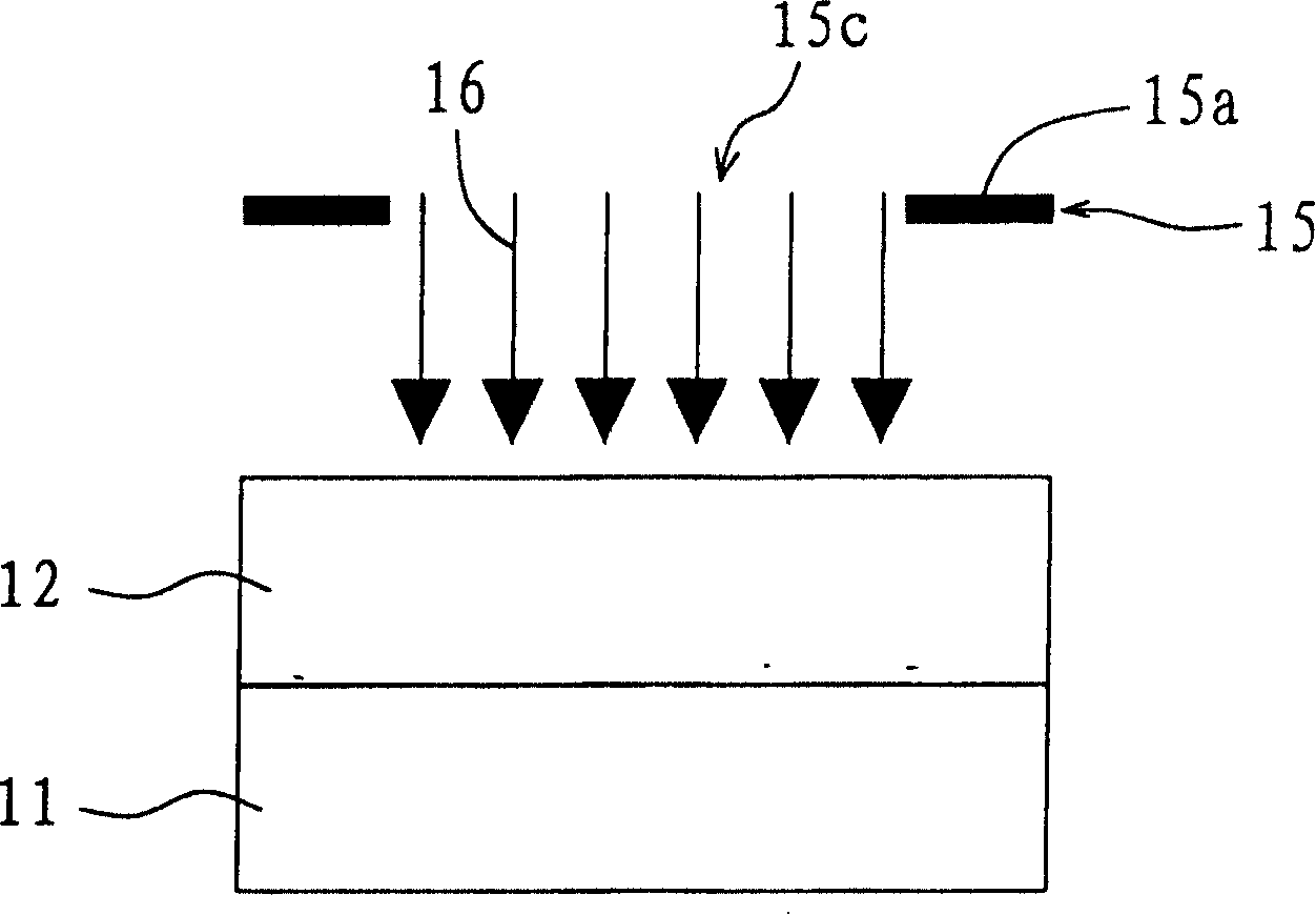
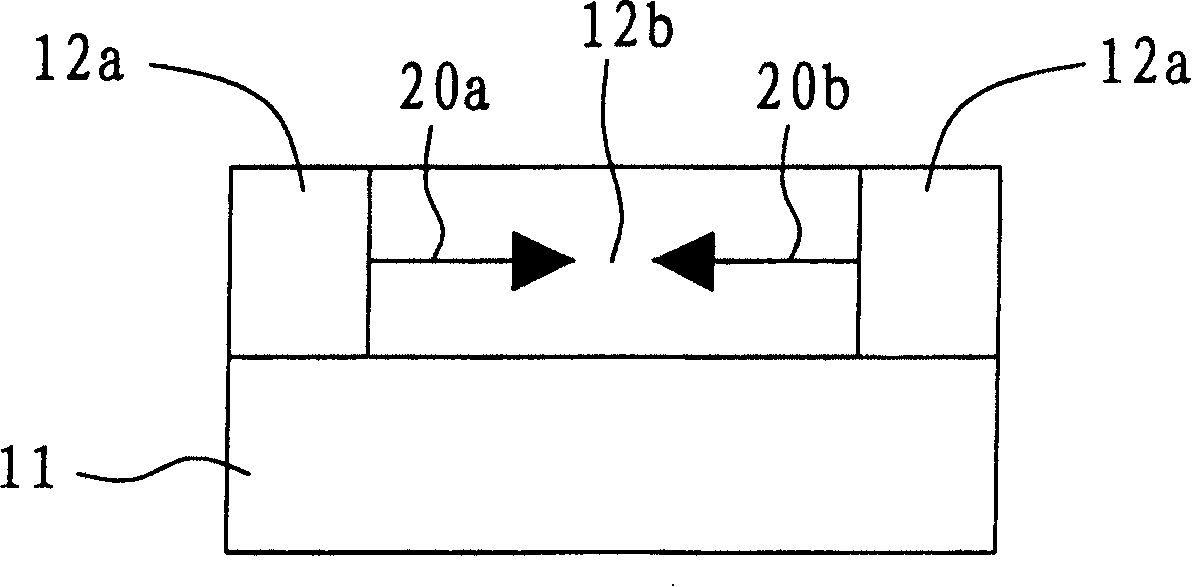
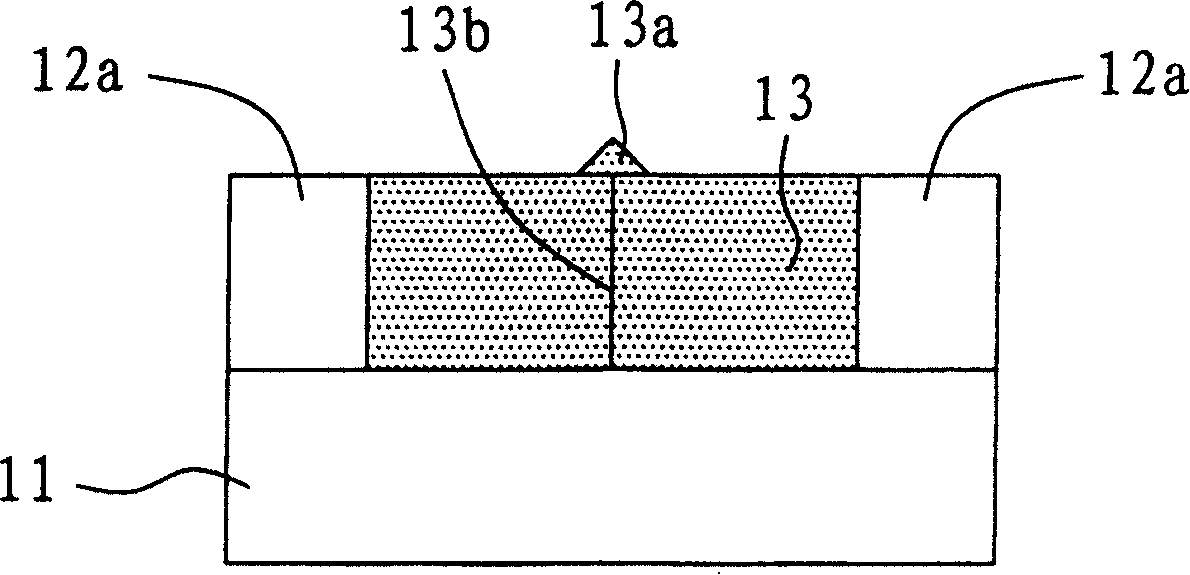
A polysilicon layer and amorphous silicon layer technology, applied in the field of photomasks, can solve the problems of increasing process steps and process costs, and low utilization rate of laser light 16
- Summary
- Abstract
- Description
- Claims
- Application Information
AI Technical Summary
Problems solved by technology
Method used
Image
Examples
Embodiment 1
[0015] Please refer to figure 2 and Figure 3A-3E , figure 2 is a flowchart of a method for manufacturing a polysilicon layer according to Embodiment 1 of the present invention, Figures 3A to 3E is a cross-sectional flow diagram of a method for manufacturing a polysilicon layer according to Embodiment 1 of the present invention. First, in step 21, a substrate 21 is provided, such as Figure 3A shown. Next, enter figure 2 In step 22, an amorphous silicon layer 32 is formed on the substrate 31, the amorphous silicon layer 32 has at least a first amorphous silicon region 32a and a second amorphous silicon region 32b, such as Figure 3B shown. Then, enter step 23, fully melt the first amorphous silicon region 32a and preheat the second amorphous silicon region 32b, as Figure 3C Shown; The first amorphous silicon region 32a that is fully melted is crystallized into a first polysilicon layer 33a, as Figure 3D shown.
[0016] In order to achieve the purpose of fully me...
Embodiment 2
[0023] Please refer to FIG. 5 , which is a top view of a photomask for preheating and melting an amorphous silicon layer by laser light according to Embodiment 2 of the present invention. In FIG. 5, the photomask 55 is used for preheating and melting an amorphous silicon layer on a substrate for a laser light. The amorphous silicon layer has a first amorphous silicon region and a second amorphous silicon region. The cover 55 moves relative to the substrate. The techniques of forming the amorphous silicon layer on the substrate and moving the photomask relative to the substrate in this embodiment have been disclosed in Embodiment 1, and will not be repeated here. The photomask 55 includes a photomask body 55b, an opaque area 55a, a first photomask pattern 56, a second photomask pattern 57 and a second part of the translucent area 55d, the opaque area 55a is formed on on the mask body 55b. The first mask pattern 56, the second mask pattern 57 and the second partial light-trans...
PUM
 Abstract
Description
Claims
Application Information


