Semiconductor memory device
A technology of storage devices and semiconductors, applied in the direction of semiconductor devices, semiconductor/solid-state device manufacturing, static memory, etc., can solve problems such as not considering the active current, not considering the reduction of consumption current, and destroying the data of the storage unit
- Summary
- Abstract
- Description
- Claims
- Application Information
AI Technical Summary
Problems solved by technology
Method used
Image
Examples
Embodiment 1
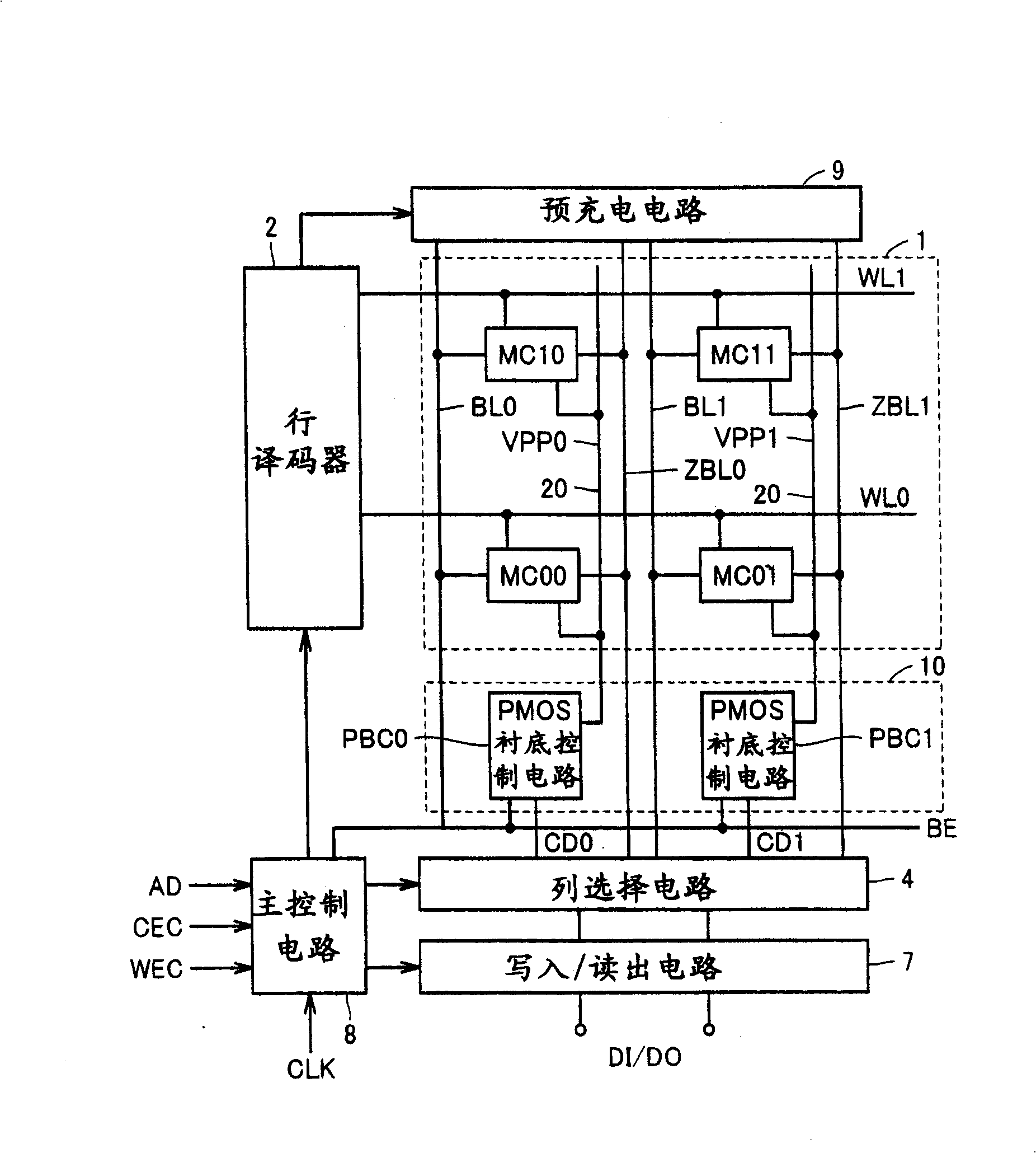
[0057] figure 1 It is an exemplary diagram schematically showing the overall structure of the semiconductor memory device of the present invention. exist figure 1 In , the structure of a synchronous single-port SRAM that operates synchronously with a clock signal is shown as an example. The configuration of the SRAM is not limited thereto, and may be an SRAM that operates in accordance with a chip select signal asynchronously with a clock signal, or may be a dual-port SRAM.
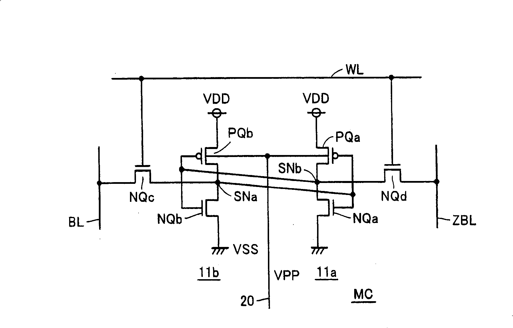
[0058] exist figure 1 Among them, the semiconductor storage device includes: a memory cell array 1 having a plurality of memory cells arranged in rows and columns; a row decoder 2 that decodes a given row address signal to generate a word line selection signal; Y address signal decoding generates the column selection signal CD for selecting the column of the memory cell array 1, and the column selection circuit 4 connecting the selection column to the internal data line; the column selected by the colu...
Embodiment 2
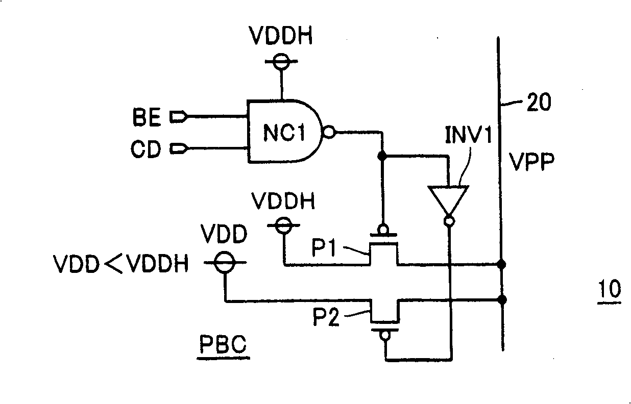
[0101] Figure 5 It is a configuration diagram showing a PMOS substrate control circuit PBC according to the second embodiment of the present invention. Should Figure 5 The structure of the PMOS substrate control circuit PBC shown is the same as image 3 The PMOS substrate control circuit PBC shown is different in the following points. That is, P-channel MOS transistor (pass transistor) P1 is coupled to a power supply node that supplies power supply voltage VDD, and pass transistor P2 is coupled to low voltage source node VDDL. Should Figure 5 Another structure of the PMOS substrate control circuit PBC shown is the same as image 3 The PMOS substrate control circuit PBC shown has the same structure, and corresponding parts are denoted by the same reference numerals, and detailed description thereof will be omitted.
[0102] The overall structure of the semiconductor memory device and figure 1 The structure of the semiconductor memory device shown is the same, in additi...
Embodiment 3
[0112] Figure 7 It is a configuration diagram showing a PMOS substrate control circuit PBC according to the third embodiment of the present invention. in the Figure 7 In the shown structure of the substrate control circuit PBC, the pass transistor P1 transmits the power supply voltage VDD to the substrate voltage transmission line according to the output signal of the NAND circuit NC1. The pass transistor P2 is coupled to the power supply VDD through the P-channel MOS transistor P3 connected as a diode, and transmits the transmitted voltage VDD-Vtp to the substrate through the P-channel MOS transistor P3 according to the output signal of the inverter INV1 voltage transmission line. Here, Vtp represents the absolute value of the threshold voltage of the P-channel MOS transistor P3.
[0113] When the high voltage of the substrate bias voltage VPP is the power supply voltage VDD, which is 1.0V, the absolute value Vtp of the threshold voltage of the P-channel MOS transistor P...
PUM
 Abstract
Description
Claims
Application Information


