Semiconductor memory device

A technology of storage devices and semiconductors, applied in the direction of semiconductor devices, semiconductor/solid-state device manufacturing, static memory, etc., can solve the problems of static noise margin reduction, storage unit data destruction, reduction, etc.

Inactive Publication Date: 2004-11-03
RENESAS ELECTRONICS CORP
View PDF5 Cites 15 Cited by
  • Summary
  • Abstract
  • Description
  • Claims
  • Application Information

AI Technical Summary

Problems solved by technology

As in the structure of Patent Document 2, at the beginning of the data writing operation, when the substrate potential is controlled to reduce the current driving capability of the drive transistor, the static noise margin is reduced, and it is not suitable for data writing.
However, even in the memory cells of the non-selected column of the selected row, the storage node is connected to the corresponding bit line, in the substrate control that reduces the current driving capability of the drive transistor in units of memory cell rows, the non-selected column of the selected row The static noise margin of the storage cells in the selected column is also reduced, and the data of the storage cells in the non-selected column is destroyed, which may cause malfunction
[0012] In addition, in any of the prior art, although the reduction of the consumption current during standby is considered, the reduction of the active current due to the charge and discharge of the bit line during operation is not considered.
[0013] In addition, in Patent Documents 3 to 5, only the layout of the memory cell array is considered, and circuit characteristics such as reduction of current consumption are not considered.

Method used


Image

  • Semiconductor memory device
  • Semiconductor memory device
  • Semiconductor memory device

Examples


Embodiment 1

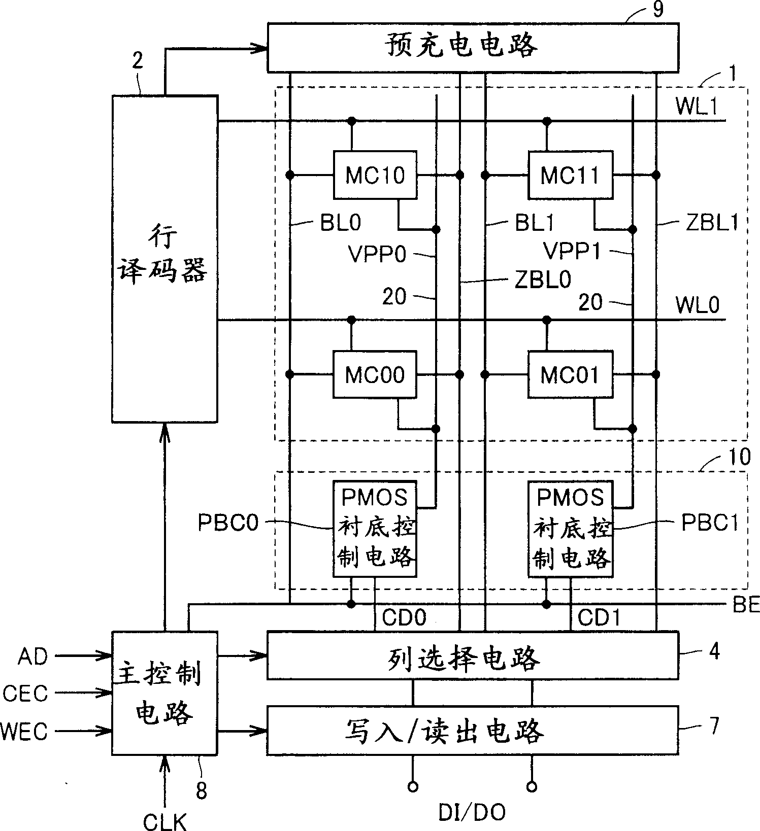
[0057] figure 1 It is an exemplary diagram schematically showing the overall structure of the semiconductor memory device of the present invention. exist figure 1 In , the structure of a synchronous single-port SRAM that operates synchronously with a clock signal is shown as an example. The configuration of the SRAM is not limited thereto, and may be an SRAM that operates in accordance with a chip select signal asynchronously with a clock signal, or may be a dual-port SRAM.

[0058] exist figure 1 Among them, the semiconductor storage device includes: a memory cell array 1 having a plurality of memory cells arranged in rows and columns; a row decoder 2 that decodes a given row address signal to generate a word line selection signal; Y address signal decoding generates the column selection signal CD for selecting the column of the memory cell array 1, and the column selection circuit 4 connecting the selection column to the internal data line; the column selected by the colu...

Embodiment 2

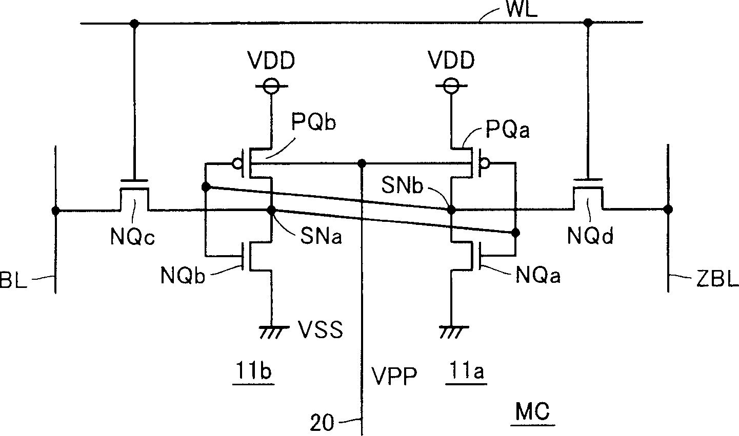
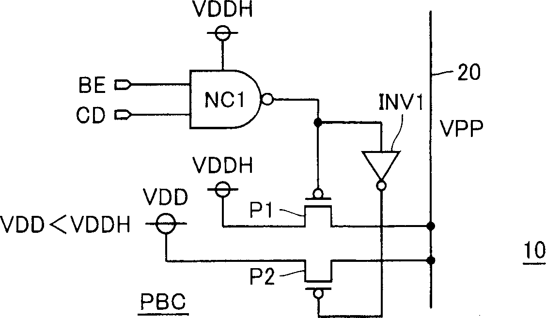
[0101] Figure 5 It is a configuration diagram showing a PMOS substrate control circuit PBC according to the second embodiment of the present invention. Should Figure 5 The structure of the PMOS substrate control circuit PBC shown is the same as image 3 The PMOS substrate control circuit PBC shown is different in the following points. That is, P-channel MOS transistor (pass transistor) P1 is coupled to a power supply node that supplies power supply voltage VDD, and pass transistor P2 is coupled to low voltage source node VDDL. Should Figure 5 Another structure of the PMOS substrate control circuit PBC shown is the same as image 3 The PMOS substrate control circuit PBC shown has the same structure, and corresponding parts are denoted by the same reference numerals, and detailed description thereof will be omitted.

[0102] The overall structure of the semiconductor memory device and figure 1 The structure of the semiconductor memory device shown is the same, in additi...

Embodiment 3

[0112] Figure 7 It is a configuration diagram showing a PMOS substrate control circuit PBC according to the third embodiment of the present invention. in the Figure 7 In the shown structure of the substrate control circuit PBC, the pass transistor P1 transmits the power supply voltage VDD to the substrate voltage transmission line according to the output signal of the NAND circuit NC1. The pass transistor P2 is coupled to the power supply VDD through the P-channel MOS transistor P3 connected as a diode, and transmits the transmitted voltage VDD-Vtp to the substrate through the P-channel MOS transistor P3 according to the output signal of the inverter INV1 voltage transmission line. Here, Vtp represents the absolute value of the threshold voltage of P-channel MOS transistor P3.

[0113] When the high voltage of the substrate bias voltage VPP is the power supply voltage VDD, which is 1.0V, the absolute value Vtp of the threshold voltage of the P-channel MOS transistor P3 is...


PUM


Abstract

A substrate potential setting circuits are provided which control substrate potentials in units of columns of a memory cell array at least in data writing. Upon data writing, the potential of the substrate region of memory cell transistors on a selected column is changed to reduce the data holding characteristics (static noise margin) to ensure high-speed data writing to the memory cells. Data writing is performed at high speed without impairing stability of data retention.

Description

technical field [0001] The present invention relates to a semiconductor memory device, and more particularly to a structure of a memory cell array portion of a static type memory (SRAM (Static Random Access Memory)) that operates statically. More specifically, the present invention relates to a structure of an SRAM capable of stably writing and reading data with low current consumption. Background technique [0002] As a method of speeding up the operation speed of a MOS transistor, there is a method of reducing the absolute value of its threshold voltage. When the absolute value of the threshold voltage decreases, the leakage current can be increased, and the internal node can be charged and discharged at high speed. [0003] However, when the absolute value of the threshold voltage decreases, there is a problem in that the leakage current (subthreshold current) between the source and the drain in the off state increases, and the consumption current increases. Various pro...

Claims


Application Information

Patent Timeline
Patent Type & Authority Applications(China)
IPC IPC(8): G11C11/413G11C7/10G11C11/412G11C11/4193H01L21/8244H01L27/11
CPCH01L27/1104G11C11/412H01L27/11G11C7/1078H10B10/00H10B10/12F16L15/007F16L13/10H05B3/56
Inventor 塚本康正新居浩二
Owner RENESAS ELECTRONICS CORP
Why Eureka
Try Eureka