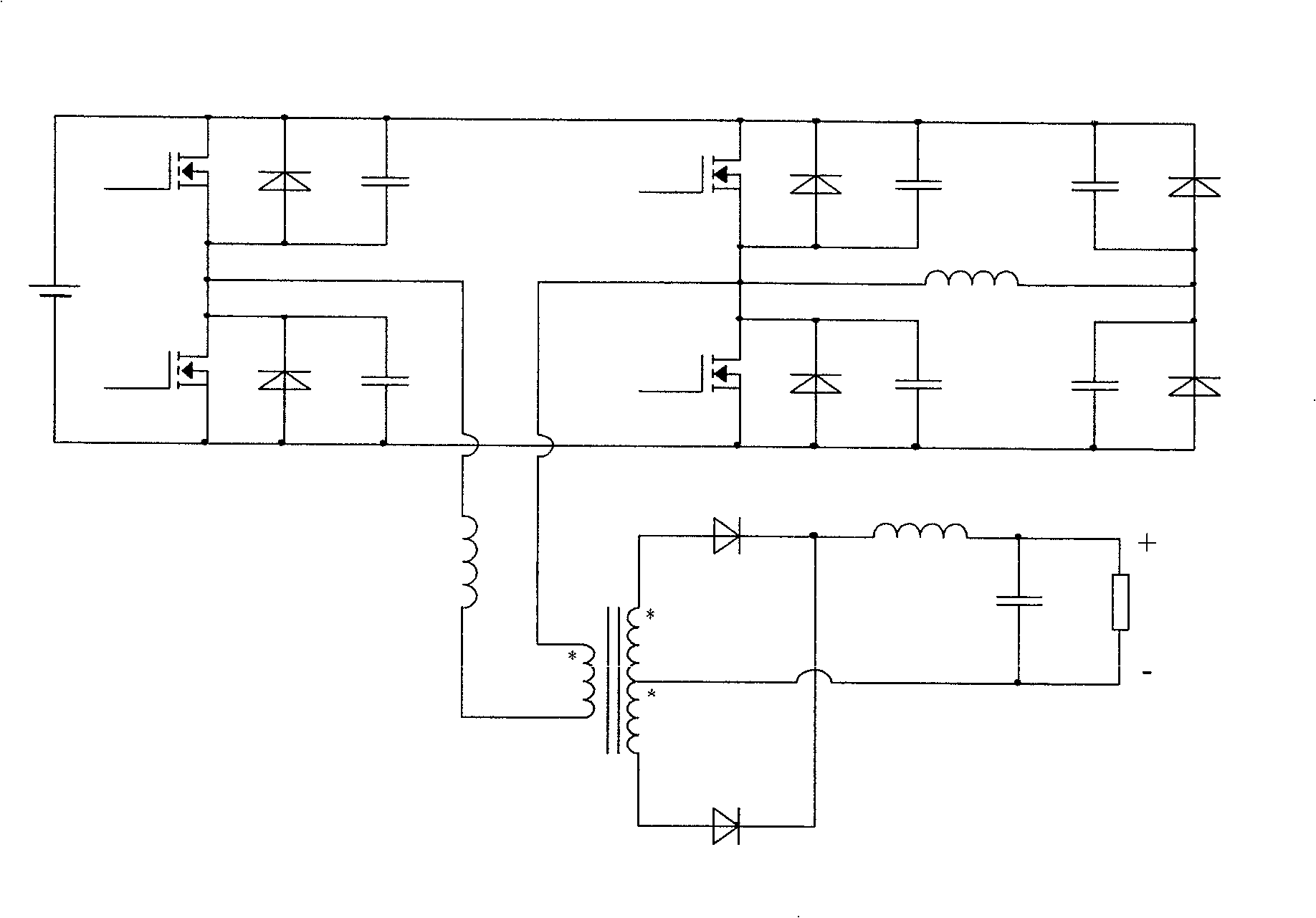
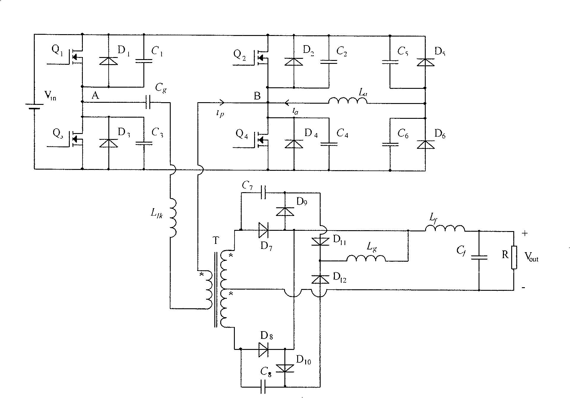
[0003] In order to solve the problem of reverse
voltage overshoot in the secondary
rectifier diode of the existing full-bridge ZVS PWM DC-
DC converter, the present invention provides a zero-voltage soft-switching full-bridge PWMDC-
DC converter with lossless buffering. The converter includes a first insulated gate
field effect transistor Q 1 , the second insulated gate
field effect transistor Q 2 , the third insulated gate
field effect transistor Q 3 , the fourth insulated gate
field effect transistor Q 4 , the first
diode D 1 , the first
capacitance C 1 , the second diode D 2 , the second
capacitance C 2 , the third diode D 3 , the third
capacitor C 3 , the fourth diode D 4 , the fourth
capacitor C 4 , the fifth diode D 5 , the fifth capacitor C 5 , the sixth diode D 6 , the sixth
capacitance C 6 ,
high frequency transformer T, seventh diode D 7 , the eighth diode D 8 , the first
inductance L a , the second
inductance L f , the third
inductance L Ik ,
filter capacitor C f and
load resistance R; the first insulated gate
field effect transistor Q 1 , the second insulated gate
field effect transistor Q 2 , the third insulated gate field effect transistor Q 3 and the fourth insulated gate field effect transistor Q 4 Constitute a full-bridge DC-DC conversion circuit, the first diode D 1 The two ends are connected in parallel to the first insulated gate field effect transistor Q 1 between the drain and source terminals, the first capacitor C 1 in parallel with the first diode D 1 both ends of the second diode D 2 The two ends of each are connected in parallel with the second insulated gate field effect transistor Q 2 between the drain and source terminals, the second capacitor C 2 in parallel with the second diode D 2 Both ends of the third diode D 3 The two ends of each are connected in parallel with the third insulated gate field effect transistor Q 3 between the drain and source terminals, a third capacitor C 3 in parallel with the third diode D 3 Both ends of the fourth diode D 4 Both ends of are connected in parallel with the fourth insulated gate field effect transistor Q 4 between the drain and source terminals, the fourth capacitor C 4 in parallel with the fourth diode D 4 The two ends; the second insulated gate field effect transistor Q 2 The source terminal of the fourth insulated gate field effect transistor Q 4 The drain terminal of is connected and this connected terminal B passes through the first inductance L a Connect the fifth diode D 5 The positive terminal and the sixth diode D 6 The negative terminal of the fifth diode D 5 The negative terminal is connected to the second insulated gate field effect transistor Q 2 The drain terminal of the sixth diode D 6 The positive terminal is connected to the fourth insulated gate field effect transistor Q 4 source terminal, the fifth capacitor C 5 in parallel with the fifth diode D 5 Both ends of the sixth capacitor C 6 Parallel to the sixth diode D 6 The two ends; the second insulated gate field effect transistor Q 2 The source end of the high-frequency
transformer T is connected to the end of the same name of the primary winding, and the third inductance L Ik One end of the high-frequency
transformer T is connected to the non-identical end of the primary winding, and the same-name end of the secondary winding of the high-frequency transformer T is connected to the seventh diode D 7 The positive terminal of the seventh diode D 7 The negative terminal is connected to the second
inductor L f One end and the eighth diode D 8 The negative terminal of the eighth diode D 8 The positive end of the high-frequency transformer T is connected to the non-identical end of the secondary winding, and the second
inductor L f The
filter capacitor C is connected in parallel between the other end of the
high frequency transformer T and the middle tap of the secondary winding f ,
filter capacitor C f The two ends of the
load resistance R are connected in parallel; the converter also includes a seventh capacitor C 7 , the eighth capacitor C 8 , the ninth capacitor C g , the ninth diode D 9 , the tenth diode D 10 , the eleventh diode D 11 , the twelfth diode D 12 and the fourth inductance L g , the first insulated gate field effect transistor Q 1 The source terminal of the third insulated gate field effect transistor Q 3 The drain terminal of the connected terminal A is connected to the third inductance L Ik There is a ninth capacitor C connected in series between the other end of g , the seventh diode D 7 The positive terminal of the seventh capacitor C is connected 7 One end of the seventh capacitor C 7 The other end of the ninth diode D is connected 9 the negative terminal of the eleventh diode D 11 positive terminal of the ninth diode D 9 The positive terminal of the seventh diode D is connected 7 The negative terminal of the eighth diode D 8 the negative terminal of the tenth diode D 10 The positive terminal of the tenth diode D 10 The negative terminal is connected to the twelfth diode D 12 The positive terminal and the eighth capacitor C 8 One end of the eighth capacitor C 8 The other end is connected to the eighth diode D 8 The positive terminal of the eleventh diode D 11 The negative terminal is connected to the fourth
inductor L g One end and the twelfth diode D 12 The negative terminal, the fourth inductor L g The other end is connected to the seventh diode D 7 negative end of

