Substrate transport container

A technology for substrates and containers, applied in the field of substrate transfer containers, can solve problems such as inability to use

Inactive Publication Date: 2009-01-07
EBARA CORP
View PDF6 Cites 1 Cited by
  • Summary
  • Abstract
  • Description
  • Claims
  • Application Information

AI Technical Summary

Problems solved by technology

Instead, by controlling the processing environment, opportunities arise to employ these materials, which were not available in the past

Method used


Image

  • Substrate transport container
  • Substrate transport container
  • Substrate transport container

Examples


Embodiment Construction

[0041] Preferred embodiments will be described below with reference to the accompanying drawings.

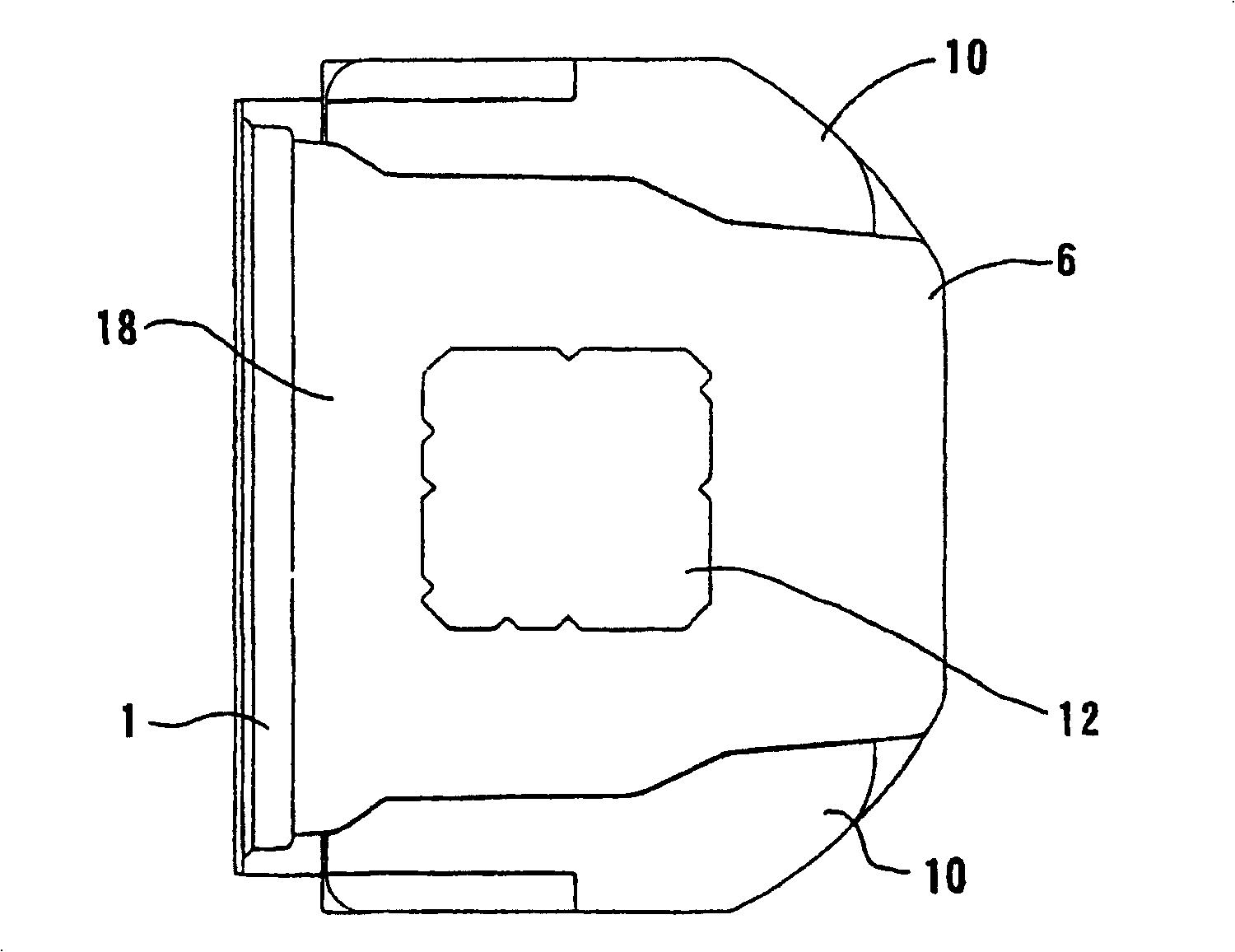
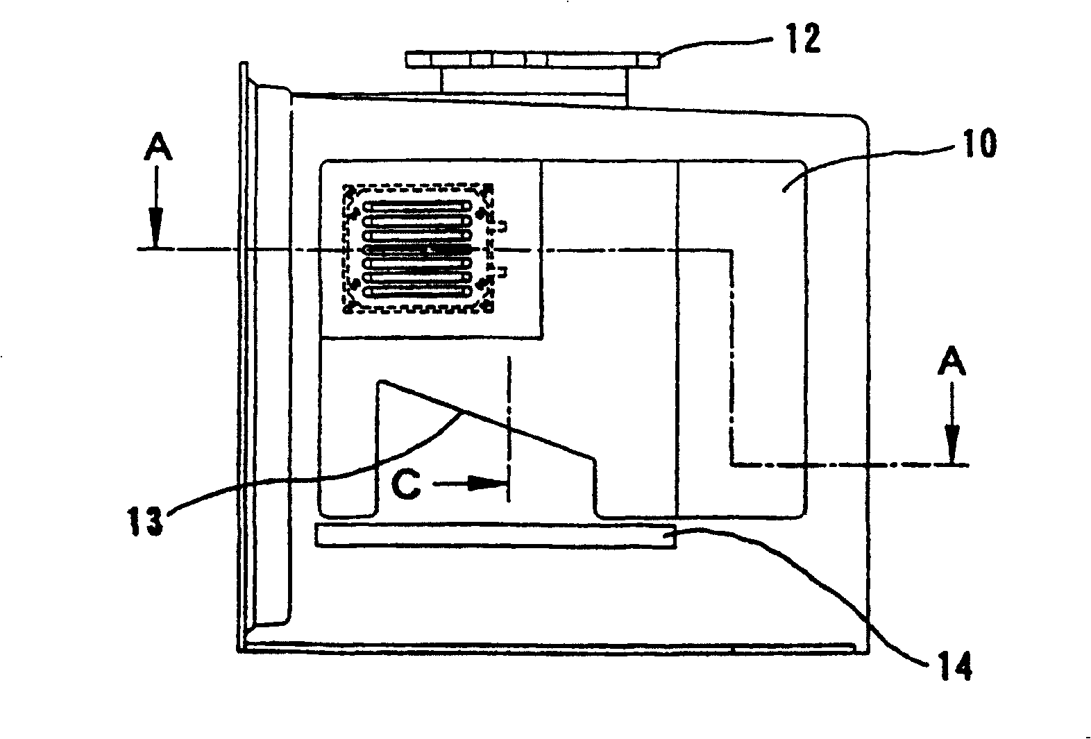
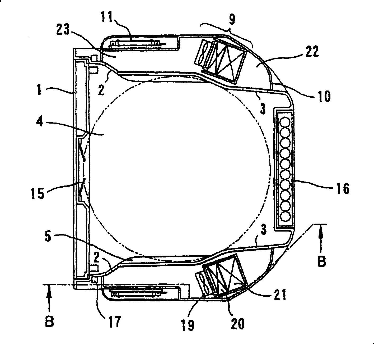
[0042] First, it is necessary to introduce a substrate transfer container (cassette) compatible with automatic operation of semiconductor device manufacturing equipment. In order to prevent human errors caused by operators and contamination of substrates such as semiconductor wafers with organic substances and trace amounts of ammonia gas generated by operators, it is effective to keep operators at a distance from a space for handling substrates. Therefore, there is a need to introduce process automation as a means of contamination for achieving this prevention. Substrate transfer containers used in such automated equipment include SMIF (Standard Mechanical Interface) containers and FOUP (Front Opening Unified Containers), which are used in combination with a door opening tool that sets the equipment at a special position and opens the door to the outside, and For use with auto...


PUM


Abstract

This invention provides a substrate transport container for use, for example, in the process of manufacturing integrated circuits of less than 0.13 mm line width, to enable to hold the level of contaminants in the interior of the container for at least particles, acidic gases, basic gases, organic substances and humidity at controlled low levels, and having the size and structure to be compatible with automated semiconductor manufacturing plants. The container is provided with a door (1) for loading and unloading substrates on a surface of a container main body and is constructed so as to hold the substrates inside the container main body at a given distance of separation, wherein air conditioning apparatuses for reducing the levels of particulate and gaseous contaminants, are disposed roughly symmetrically on the container main body (6).

Description

technical field [0001] The present invention relates to structures, capabilities and methods of operating a substrate transfer container suitable for storing or transferring objects, such as semiconductor wafers, photomasks or hard disks, in a highly clean environment. Background technique [0002] As the pattern size of semiconductor devices becomes finer, even higher cleanliness will be expected in the future. For example, the target control size of particulate contaminants that may cause pattern defects and wiring shorts should be considered in advance to be less than 0.1 μm. Furthermore, gaseous pollutants must be reduced in addition to particulate pollutants. By being absorbed onto the semiconductor wafer, various hydrocarbon molecules cause a drop in the insulation breakdown voltage of the gate oxide film or a change in the thickness in the deposited film, and the alkaline gas reacts with the chemically amplified photoresist, resulting in resolution loss, acid gas ma...

Claims


Application Information

Patent Timeline
IPC IPC(8): H01L21/00B65D85/86B01D53/26H01L21/673
CPCH01L21/67393H01L21/68
Inventor 田中亮铃木庸子岸贵士
Owner EBARA CORP
Why Eureka
Try Eureka