Semiconductor device
A semiconductor and chip technology, applied in the direction of semiconductor devices, semiconductor/solid-state device parts, electric solid-state devices, etc., can solve complex problems such as combination processing
- Summary
- Abstract
- Description
- Claims
- Application Information
AI Technical Summary
Problems solved by technology
Method used
Image

Examples
no. 1 example
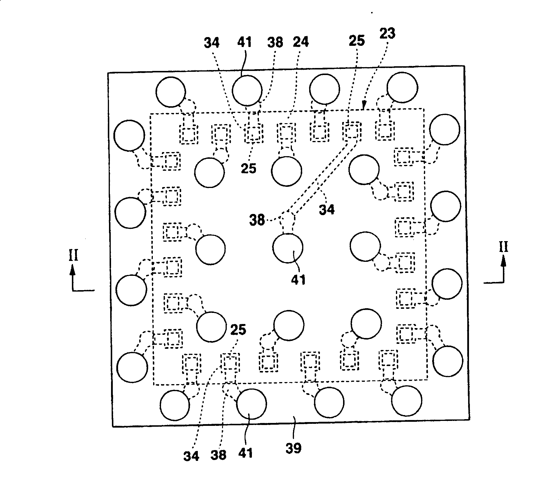
[0061] figure 1 is a plan view showing a semiconductor device according to a first embodiment of the present invention, figure 2 is along figure 1 Sectional view along line II-II shown in . at this time, figure 1 and figure 2 The difference is that the dimensions of the individual elements of the semiconductor device are not equal to each other.
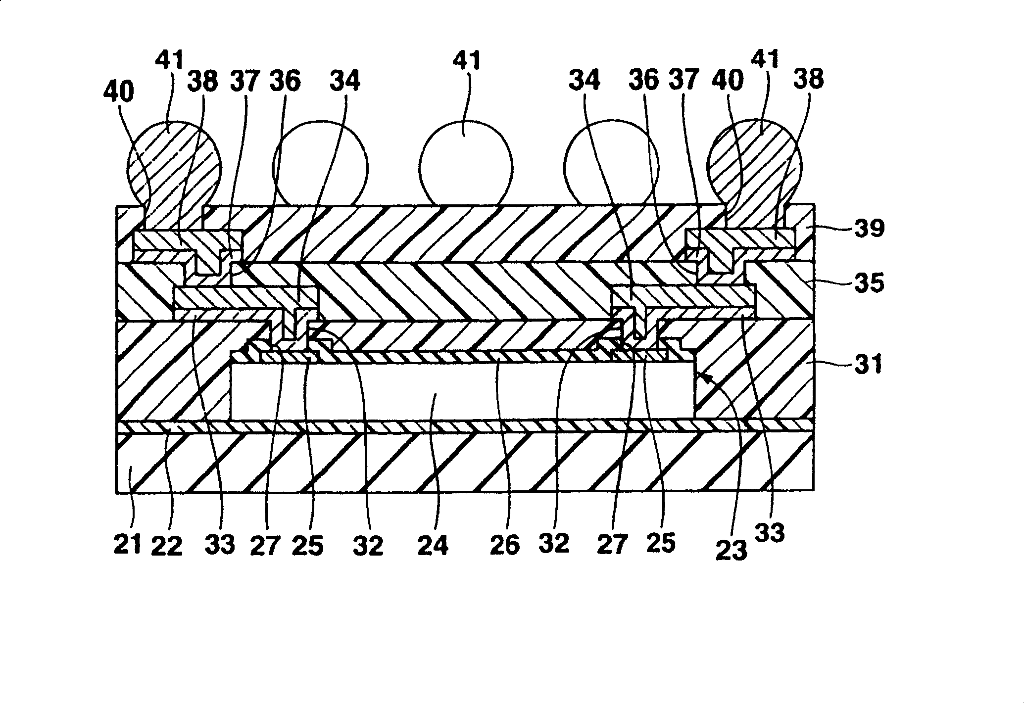
[0062] This semiconductor device includes a square substrate 21 made of, for example, a resin plate, a metal plate, or a glass plate. An adhesive layer 22 made of, for example, an adhesive, an adhesive sheet, or a double-coated tape is formed on the entire upper surface of the substrate 21 . The lower surface of a silicon substrate 24 of a substantially square semiconductor chip 23 , which is slightly smaller in size than the substrate 21 , is mounted on the central portion of the upper surface of the adhesive layer 22 .
[0063] The semiconductor chip 23 includes a plurality of connection pads 25 made of, for example, alu...
no. 2 example
[0085] Figure 12 is a vertical sectional view showing a semiconductor device according to a second embodiment of the present invention. Figure 12 The semiconductor device shown in the figure 2 There are significant differences in the semiconductor devices shown in Figure 12 In the shown semiconductor device, the pad portion of the first rewiring 34 is connected to the pad portion of the second rewiring 34 through the columnar electrode arranged in the opening portion 36 formed in the portion of the second insulating film 35 above the pad. The second underlying metal layer 37 below the wiring 38 .
[0086] Now explain the manufacture Figure 12 Exemplary methods of semiconductor devices shown. In this case, those manufacturing steps up to the step of peeling off the corrosion-resistant plating film 51 as shown in FIG. 4 are the same as those of the first embodiment of the present invention described above. Therefore, the subsequent manufacturing steps will be described...
no. 3 example
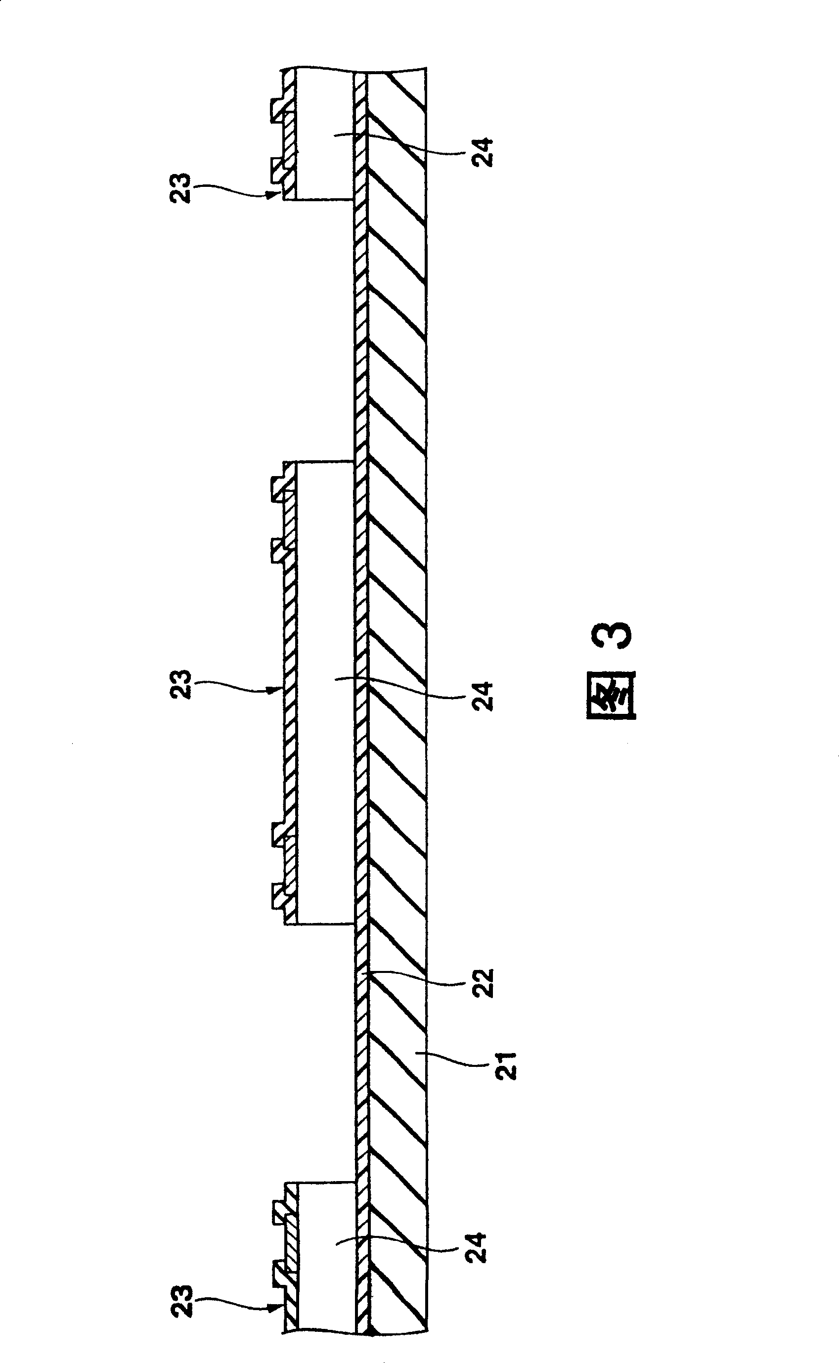
[0097] When in the manufacturing steps shown in FIG. 3, the adhesive layer 22 is formed only on the lower surface of the silicon substrate 24 of the semiconductor chip 23, and is bonded to a predetermined position on the upper surface of the substrate 21, the third The semiconductor device of the embodiment, such as Figure 19 shown. In order to form the adhesive layer 22 on the lower surface of the silicon substrate 24 of the semiconductor chip 23, it is effective to fix the adhesive layer 22 to the back surface of the silicon wafer on which the connection pads 25 and the insulating film 26 are formed, and then dicing This silicon wafer yields a semiconductor chip 23 with an adhesive layer 22 formed on the back thereof. Alternatively, it is also possible to drop the mold coating material on those regions on the substrate 21 where the semiconductor chip 23 is to be mounted by using such as a dispenser (dispenser), after which the semiconductor chip 23 is mounted on the mold c...
PUM
| Property | Measurement | Unit |
|---|---|---|
| thickness | aaaaa | aaaaa |
| height | aaaaa | aaaaa |
Abstract
Description
Claims
Application Information
 - R&D
- Intellectual Property
- Life Sciences
- Materials
- Tech Scout
- Unparalleled Data Quality
- Higher Quality Content
- 60% Fewer Hallucinations
Browse by: Latest US Patents, China's latest patents, Technical Efficacy Thesaurus, Application Domain, Technology Topic, Popular Technical Reports.
© 2025 PatSnap. All rights reserved.Legal|Privacy policy|Modern Slavery Act Transparency Statement|Sitemap|About US| Contact US: help@patsnap.com