Relay base plate and multilayer printed wiring board

A relay substrate, multi-layer printing technology, applied in the direction of circuits, electrical components, electrical solid devices, etc., can solve the problems of difficult to carry high frequency, high performance, high ceramic resistance value, high dielectric constant, etc.

Active Publication Date: 2009-04-08
IBIDEN CO LTD
View PDF10 Cites 1 Cited by
  • Summary
  • Abstract
  • Description
  • Claims
  • Application Information

AI Technical Summary

Problems solved by technology

Here, since the ceramic package substrate uses metallized wiring formed by firing, the resistance value of the ceramic will become higher. In addition, the dielectric constant of the ceramic is high, and it is difficult to mount a high-frequency, high-performance IC.

Method used


Image

  • Relay base plate and multilayer printed wiring board
  • Relay base plate and multilayer printed wiring board
  • Relay base plate and multilayer printed wiring board

Examples


Embodiment 1

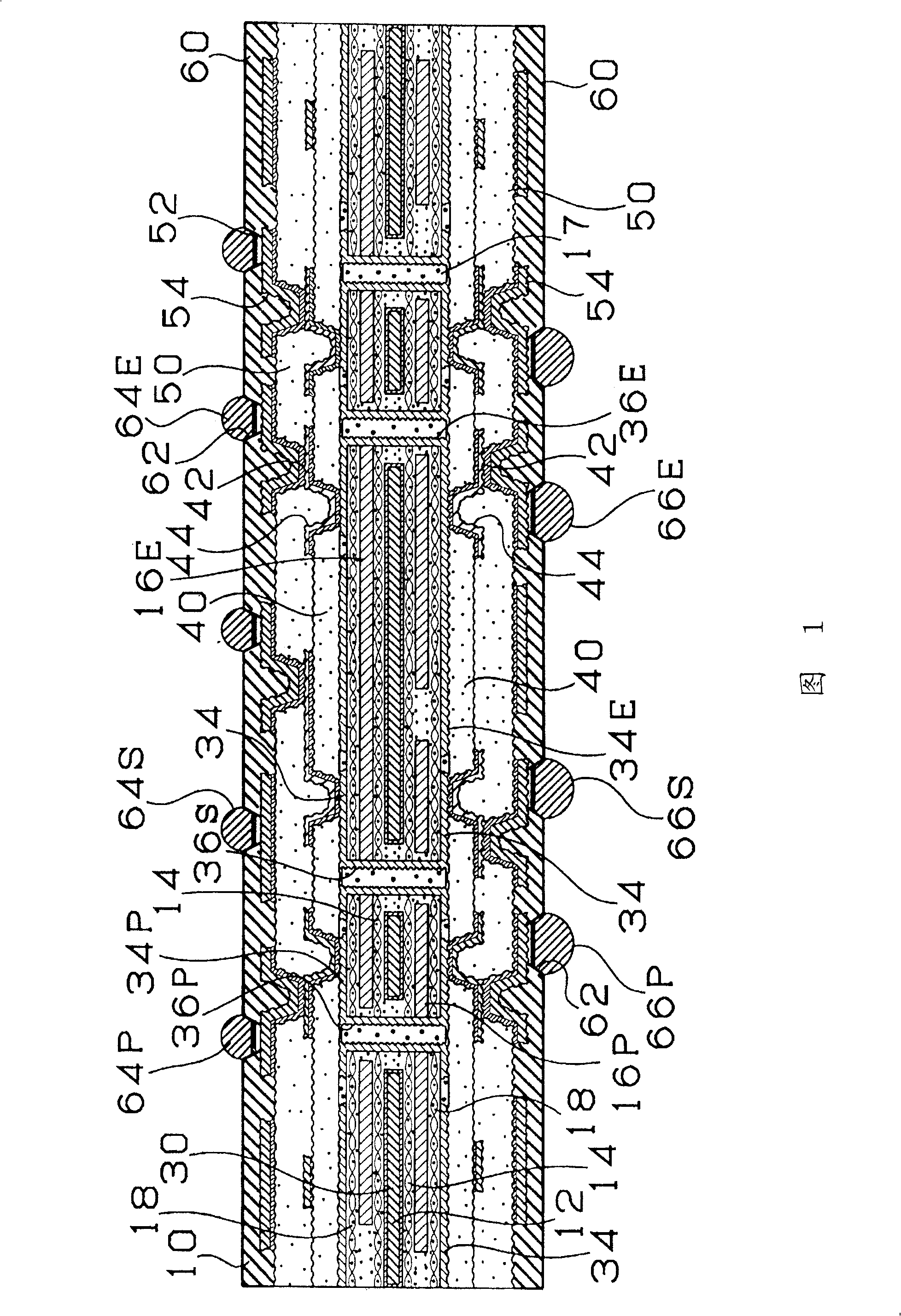
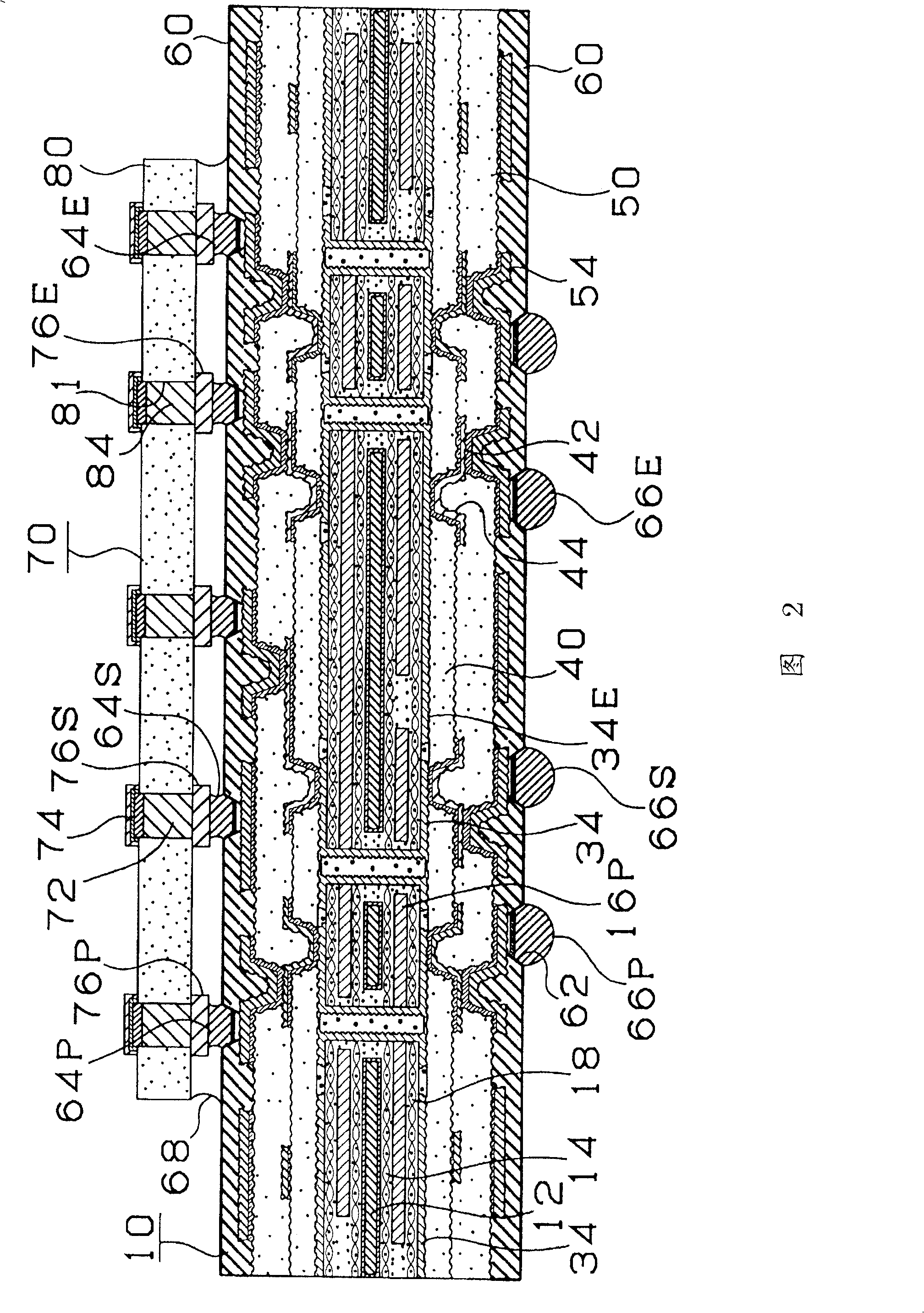
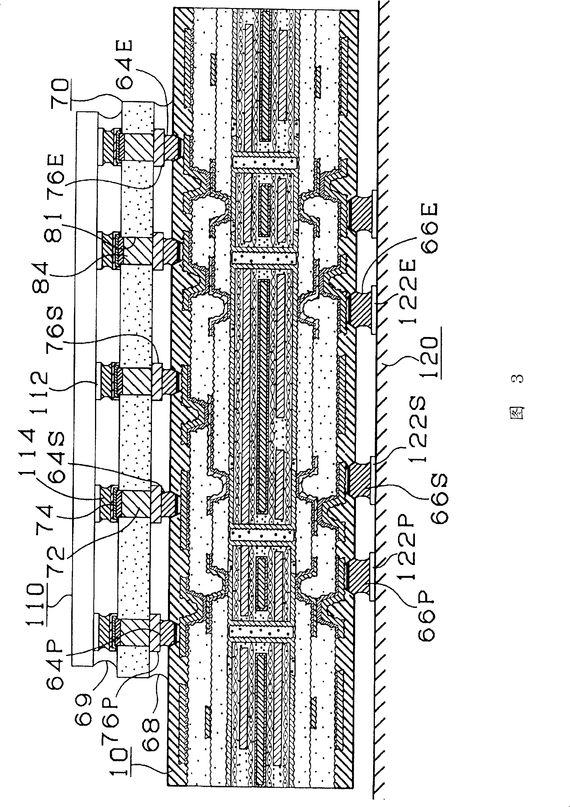
[0059]In the resin package substrate 10 of the first embodiment, the power supply capability to the IC chip 110 can be improved by using the conductor layers 34P and 16P as power supply layers. Therefore, when the IC chip 110 is mounted on the package substrate 10, the loop inductance from the IC chip 110 to the substrate 10 to the sub-board 120 side power supply can be reduced. Therefore, since the power shortage during the initial operation becomes smaller, it is less likely to cause a power shortage. Therefore, even if an IC chip in the high-frequency field is mounted, it will not cause erroneous operation or errors during the initial startup. In addition, by using the conductor layers 34E and 16E as ground layers, noise is not superimposed on the signal and power supply of the IC chip, and the occurrence of erroneous operations or errors can be prevented. In addition, by installing a capacitor not shown in the figure, the power stored in the capacitor can be used in an aux...

Embodiment 2

[0090] [Example 2] Young's modulus = 55GPa, external dimensions = 32mm × 32mm, relay substrate thickness = 64μm

[0091] For the relay substrate of Example 2, in Example 1, the substrate thickness of the starting material was set to 64 μm. Therefore, the laser conditions for forming the through holes were changed to the conditions shown in the table below. In addition, the plating time for filling the conductive agent in the through holes is changed according to the thickness of the substrate. Other than that, it was the same as Example 1.

[0092] 【Table 2】

[0093] "Laser Conditions"

[0094] Mask diameter

Embodiment 3

[0095] [Example 3] Young's modulus = 55GPa, external dimensions = 32mm × 32mm, relay substrate thickness = 100μm

[0096] For the relay substrate of Example 3, in Example 1, the substrate thickness of the starting material was set to 100 μm. Therefore, the laser conditions for forming the through holes were changed to the conditions shown in the table below. In addition, the plating time for filling the conductive agent in the through hole is changed according to the thickness of the substrate. Other than that, it was the same as Example 1.

[0097] 【table 3】

[0098] "Laser Conditions"

[0099] Mask diameter


PUM


Abstract

Disclosed is an interposer which enables to prevent breaking of wiring pattern in an IC chip mounted on a package substrate. By arranging an interposer (70) between a package substrate (10) and an IC chip (110), there can be absorbed the stress due to the difference of thermal expansion coefficient between the multilayer printed wiring board (10) having a large thermal expansion coefficient and the IC chip (110) having a small thermal expansion coefficient. In particular, by using an insulating substrate (80) having a Young's modulus of 55-440 GPa as a component of the interposer (70), the stress can be absorbed in the interposer (70).

Description

technical field [0001] The present invention relates to a relay substrate and a multilayer printed circuit board, in particular to a relay substrate provided between a packaging substrate made of resin and an IC chip made of ceramics, and a relay substrate with a connecting IC chip. Multilayer printed circuit boards for relay substrates. Background technique [0002] Package substrates are used to connect fine-pitch IC chips to external substrates such as daughter boards. The material of the package substrate is ceramic or resin. Here, the ceramic package substrate uses metallized wiring formed by firing, so the resistance value of the ceramic will become high. In addition, the dielectric constant of the ceramic is high, and it is difficult to mount high-frequency and high-performance ICs. In addition, since the resin packaging substrate uses copper wiring formed by electroplating, the wiring resistance can be reduced, and the dielectric constant of the resin is low, makin...

Claims


Application Information

Patent Timeline
Patent Type & Authority Patents(China)
IPC IPC(8): H01L23/32
CPCH01L2224/16225H01L2224/32225H01L2224/73204H01L2924/15311
Inventor 苅谷隆古谷俊树
Owner IBIDEN CO LTD
Why Eureka
Try Eureka