
Semiconductor device

A semiconductor and thin film transistor technology, applied in semiconductor devices, semiconductor/solid-state device manufacturing, transistors, etc., can solve the problem of uneven crystal grain size, and achieve the effects of excellent characteristics, reduced characteristic variation, and high yield

Inactive Publication Date: 2009-08-05
SEMICON ENERGY LAB CO LTD
View PDF4 Cites 0 Cited by
  • Summary
  • Abstract
  • Description
  • Claims
  • Application Information

AI Technical Summary

Problems solved by technology

The grain size of the crystal becomes non-uniform due to the influence of the energy distribution of the laser beam during scanning

Method used


Image

  • Semiconductor device
  • Semiconductor device
  • Semiconductor device

Examples


Embodiment approach 1

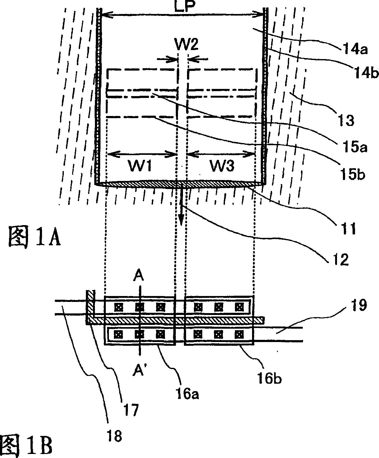
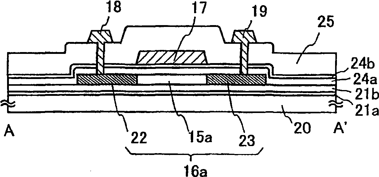
[0042] A state in which a CW laser beam is scanned on the surface of a semiconductor film formed on a substrate and a manufactured TFT will be described with reference to FIGS. 1A to 1C.

[0043] FIG. 1A is a plan view showing a scanning state of a laser beam 11 on the surface of an amorphous semiconductor film. A laser beam 11 has an elongated elliptical beam spot and is scanned in a scanning direction 12 indicated by an arrow in the figure to partially form a crystal region.

[0044] Although not shown in FIG. 1A, since the figure shows an example of forming a top gate type TFT, a base insulating film is formed over a substrate having an insulating surface and an amorphous semiconductor film is formed thereon.

[0045] In the crystallization process of an amorphous semiconductor film, a continuous wave solid-state laser is used in this embodiment mode and a laser beam having the second, third, or fourth harmonic of the fundamental wave is emitted onto the semiconductor film ...

Embodiment approach 2

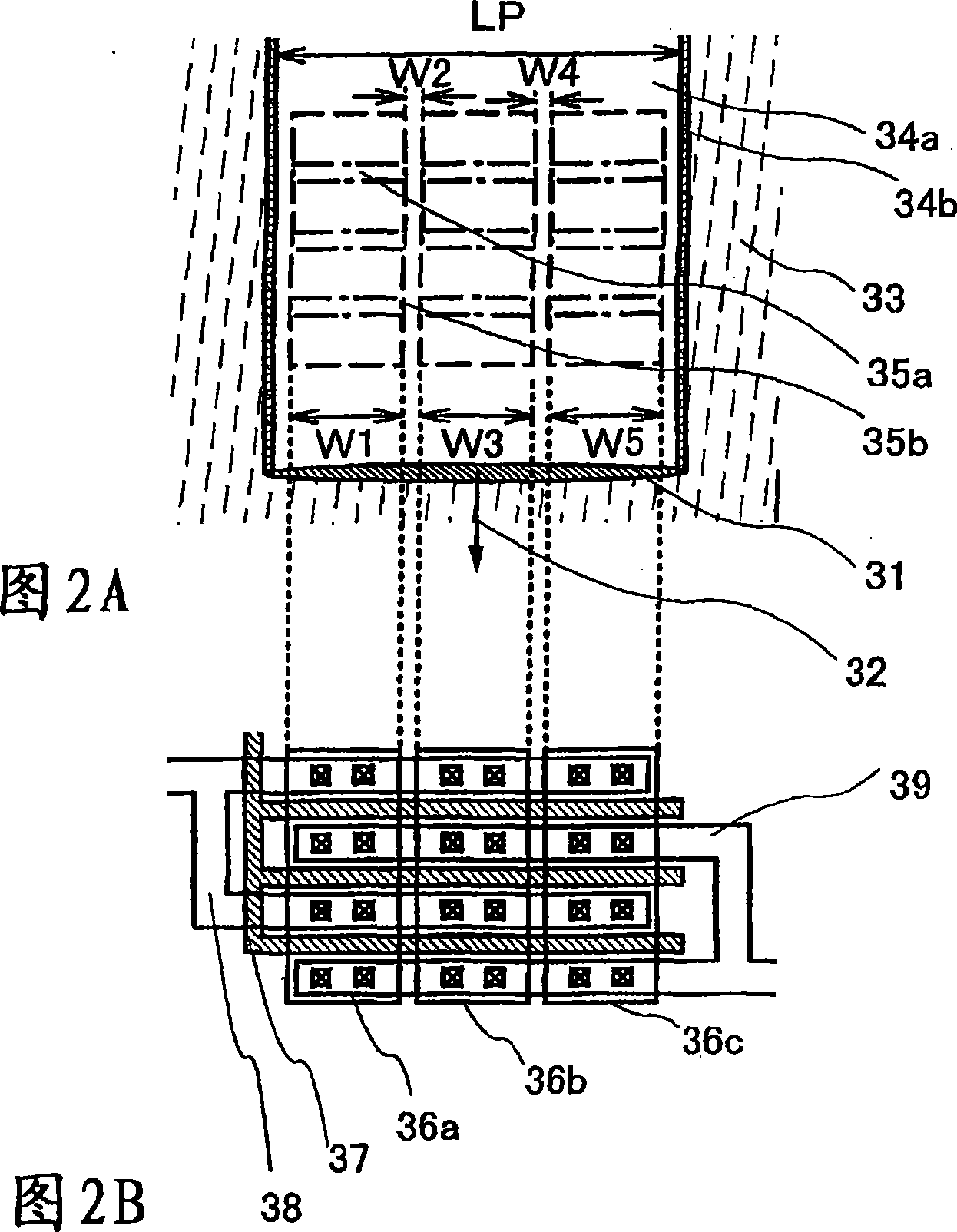
[0068] A state in which a quasi-CW laser beam is scanned on the surface of a semiconductor film formed over a substrate and a manufactured TFT are described with reference to FIGS. 2A and 2B.

[0069] FIG. 2A is a plan view showing a scanning state of a laser beam 31 on the surface of an amorphous semiconductor film. A laser beam 31 has an elongated elliptical beam spot and is scanned in a scanning direction 32 indicated by an arrow in the figure to partially form a crystal region.

[0070] Although not shown in FIG. 2A, since the figure shows an example of forming a top gate type TFT, a base insulating film is formed on a substrate having an insulating surface and an amorphous semiconductor film is formed thereon.

[0071] In the process of crystallizing the amorphous semiconductor film, YVO with an output of 1.8W was used 4 laser with a repetition rate of 80 MHz and a pulse width of approximately 12 ps. The pulse repetition rate is not limited to 80 MHz in the present inve...

Embodiment 1

[0088] In Embodiment 1, refer to image 3 The structure of the laser irradiation equipment will be described.


PUM


Abstract

When a semiconductor film is irradiated with conventional pulsed laser light, unevenness called ridges is caused on the surface of the semiconductor film. In the case of a top gate type TFT, the characteristics of the element vary depending on the ridge, specifically, there is a problem of variation among a plurality of thin film transistors electrically connected in parallel with each other. According to the present invention, when manufacturing a circuit including a plurality of thin film transistors, the width LP of the region (excluding the microcrystalline region) melted by irradiating the semiconductor film with continuous wave laser light is increased, and a plurality of thin film transistors ( active layers electrically connected in parallel with each other).

Description

technical field [0001] The present invention relates to a semiconductor device having a circuit including a thin film transistor (hereinafter referred to as TFT) and a method of manufacturing the same. For example, the present invention relates to an electronic device having an electro-optical device, typically a liquid crystal display panel or a light-emitting display device having an organic light-emitting element, as its component. [0002] A semiconductor device in this specification refers to a general device that can operate using semiconductor characteristics and includes all types of devices such as electro-optic devices, semiconductor circuits, and electronic devices. Background technique [0003] In recent years, a technique of forming a thin film transistor (TFT) using a semiconductor thin film (about several nanometers to several hundred nanometers thick) formed over a substrate having an insulating surface has attracted attention. Thin film transistors are wide...

Claims


Application Information

Patent Timeline
Patent Type & Authority Patents(China)
IPC IPC(8): H01L21/336H01L21/20H01L29/786
CPCH01L27/1285H01L21/02532H01L21/02683H01L29/78621H01L27/1296H01L21/02691H01L21/02672H01L21/02686H01L21/02667H01L21/0237
Inventor 山崎舜平田中幸一郎
Owner SEMICON ENERGY LAB CO LTD
Learn More