Substrate with embedded element and manufacturing method thereof

A manufacturing method and embedded technology, which is applied in semiconductor/solid-state device manufacturing, electrical components, printed circuit manufacturing, etc., can solve the problem of affecting the combination of the substrate and embedded components during lamination, affecting the alignment of embedded components and contacts, and the failure of components Issues such as embedding the substrate to achieve the effect of increasing space utilization, strengthening bonding, and reducing the number

Inactive Publication Date: 2009-09-16
ADVANCED SEMICON ENG INC
View PDF3 Cites 3 Cited by
  • Summary
  • Abstract
  • Description
  • Claims
  • Application Information

AI Technical Summary

Problems solved by technology

However, in the existing technology of using embedded electronic components, when the circuit layer and the insulating layer are laminated to form the substrate, since the insulating layer is mostly solid and hard to deform after being cured at high temperature, it is easy to cause the embedded components to be separated from the substrate. There are still many unfilled gaps between the insulating layers. These gaps not only easily affect the bonding between the substrate and embedded components during pressing, but also affect the alignment between embedded components and contacts during pressing.
In addition, in a circuit substrate with a single insulating layer, the thickness of the insulating layer is usually smaller than the thickness of the embedded components, which may easily cause problems such as the inability to embed the components in the substrate.

Method used


Image

  • Substrate with embedded element and manufacturing method thereof
  • Substrate with embedded element and manufacturing method thereof
  • Substrate with embedded element and manufacturing method thereof

Examples


Embodiment Construction

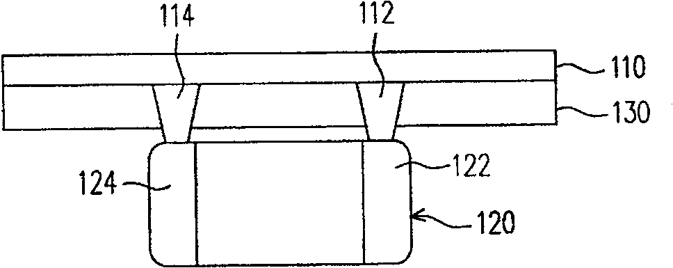
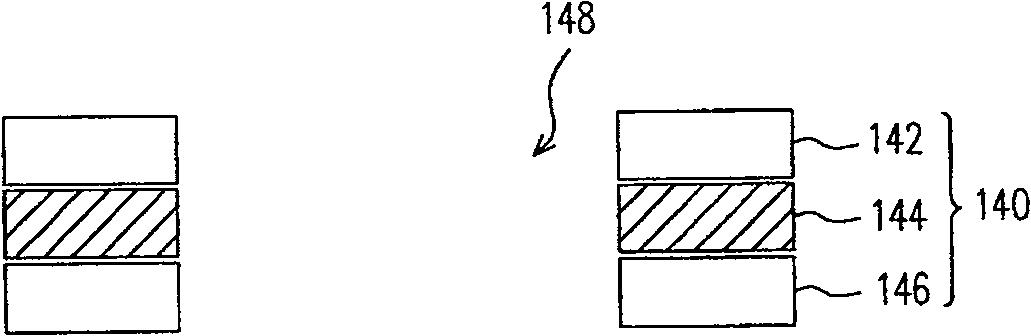
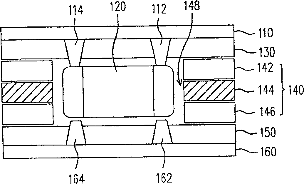
[0030] Figure 1 to Figure 5 Shown is a schematic diagram of a manufacturing method of a substrate with embedded components according to the first embodiment of the present invention. First, please refer to figure 1 , providing a first metal layer 110 and an embedding element 120 , the embedding element 120 can be welded on the two bumps 112 , 114 preformed on the first metal layer 110 by means of a hot pressing technique. Wherein, the material of the first metal layer 110 may be copper, and the two bumps 112 and 114 may be copper bumps produced by electroplating. When the two electrodes 122, 124 of the embedded component 120 are correspondingly placed on the two bumps 112, 114 of the first metal layer 110, the welding material (not shown) at the electrode end can be bonded by high temperature thermocompression, so that the first The two bumps 112 , 114 of the metal layer 110 are firmly bonded to the two electrodes 122 , 124 of the embedded element 120 . In addition, the fo...


PUM


Abstract

The invention discloses a substrate with embedded components and a manufacturing method thereof. The manufacturing method includes providing a first metal layer and an embedded component, the first metal layer has at least two first bumps, which are correspondingly connected to the embedded component; then, placing the embedded component in a buried hole in a core layer; providing A second metal layer, and the second metal layer has at least two second bumps, corresponding to the embedded element; after that, sequentially press the first metal layer, the core layer and the second metal layer, so that the two first The bump and the two second bumps are respectively electrically connected to the embedded components; finally, the first metal layer is patterned to form a first circuit layer; and the second metal layer is patterned to form a second circuit layer , and the embedded element is electrically connected between the first circuit layer and the second circuit layer.

Description

technical field [0001] The invention relates to a substrate and a manufacturing method thereof, in particular to a substrate with embedded components capable of improving the combination between a core layer and embedded components and a manufacturing method thereof. Background technique [0002] Generally speaking, a circuit substrate is mainly formed by overlapping layers of patterned circuit layers and dielectric layers alternately. Wherein, the patterned circuit layer is formed by photolithography and etching of a copper foil layer, and the insulating layer is located between the patterned circuit layers for isolating the patterned circuit layers. In addition, the overlapping patterned circuit layers are electrically connected to each other through Plating Through Holes (PTH) or conductive vias penetrating the insulating layer. Finally, arrange various electronic components (active components, passive components) on the surface of the circuit substrate, and achieve the ...

Claims


Application Information

Patent Timeline
Patent Type & Authority Patents(China)
IPC IPC(8): H05K3/30H05K3/00H01L23/498H01L21/48H01L21/60
Inventor 洪清富许武州
Owner ADVANCED SEMICON ENG INC
Why Eureka
Try Eureka