Panel display device with knot type field effect tube cathodic control array structure and its production technique

A flat-panel display and field effect tube technology, which is applied in cold cathode manufacturing, discharge tube cold cathode, control electrodes, etc., can solve the problems of different luminous degrees of light-emitting pixels, differences in emission capabilities, and adverse effects on display image quality, etc., to achieve good results. Effect of field emission characteristics, reduction of production cost, and simplification of production process

Inactive Publication Date: 2009-10-28
ZHONGYUAN ENGINEERING COLLEGE
View PDF5 Cites 0 Cited by
  • Summary
  • Abstract
  • Description
  • Claims
  • Application Information

AI Technical Summary

Problems solved by technology

Affected by various external factors, the field emission capabilities of different carbon nanotube cathodes will be different, resulting in different luminescence levels of the corresponding luminescent pixels, which will adversely affect the display image quality

Method used


Image

  • Panel display device with knot type field effect tube cathodic control array structure and its production technique
  • Panel display device with knot type field effect tube cathodic control array structure and its production technique
  • Panel display device with knot type field effect tube cathodic control array structure and its production technique

Examples


Embodiment Construction

[0041] The present invention will be further described below in conjunction with the accompanying drawings and embodiments, but the present invention is not limited to these embodiments.

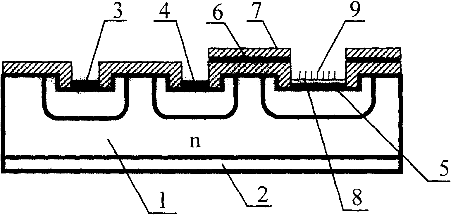
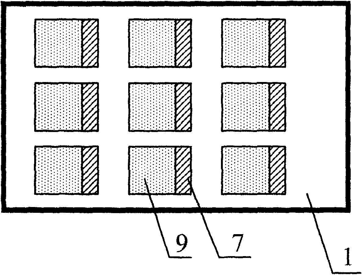
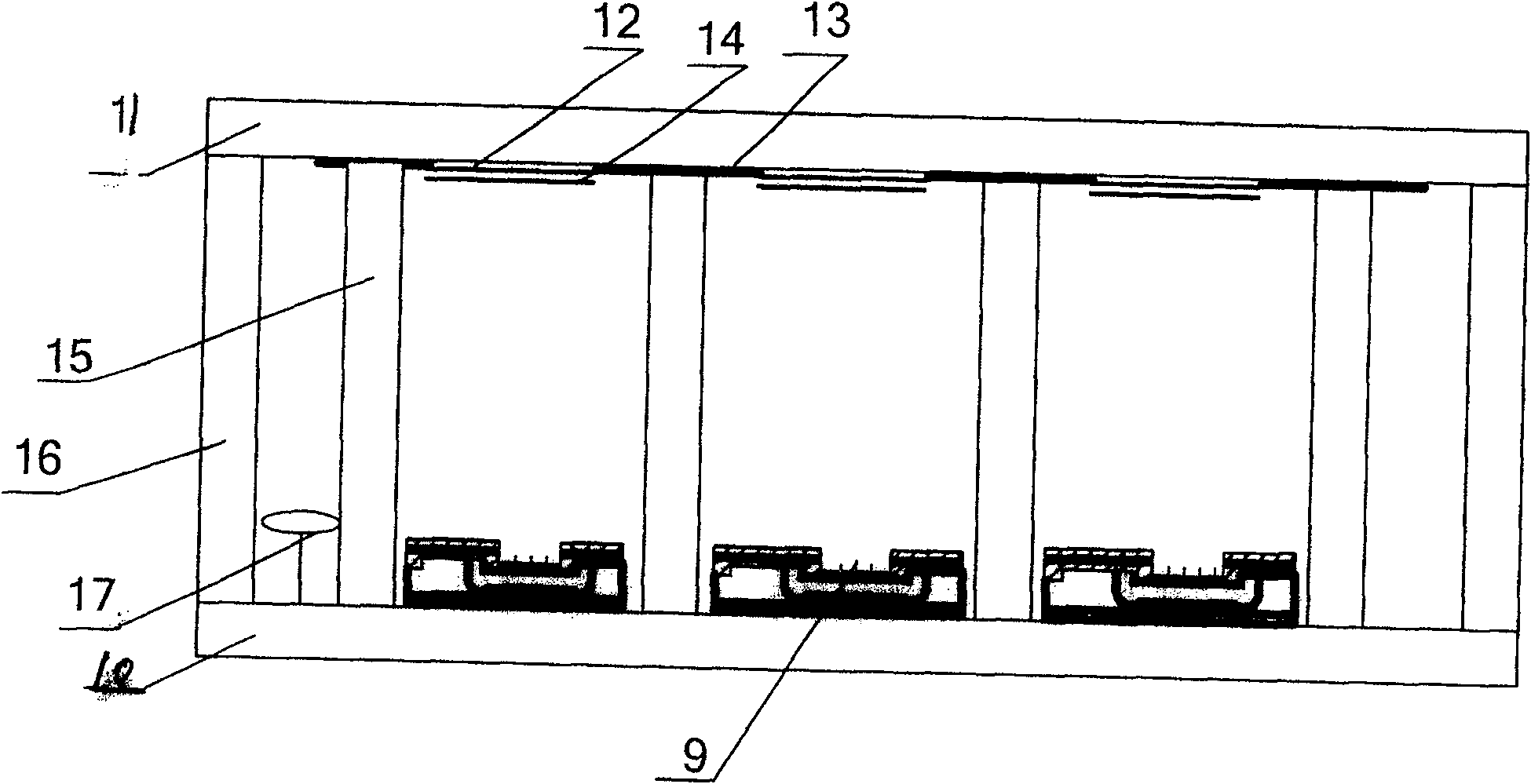
[0042] Described a kind of flat-panel display with junction field effect tube cathode control array structure, comprises the sealed vacuum cavity that is made of cathode glass panel 10, anode glass panel 11 and surrounding glass frame 16; On the anode glass panel 11 There is a photolithographic anode conductive layer 12 and a phosphor layer 14 prepared on the anode conductive layer; on the cathode glass panel 10, there are prepared carbon nanotube 9 cathodes, control grids 6 and junction field effect tube cathode control array structures ; The support wall structure 15 and the getter 17 accessory elements located between the anode glass panel and the cathode glass panel.

[0043] The junction field effect transistor cathode control array structure includes a substrate 1, a backside p-type he...


PUM


Abstract

The invention particularly relates to a flat panel display with a junction field effect tube cathode control array structure and its manufacturing process, including a sealed vacuum chamber formed by a cathode glass panel, an anode glass panel and surrounding glass frames; on the anode glass panel There is a photolithographic anode conductive layer and a phosphor layer prepared on the anode conductive layer; there are prepared carbon nanotube cathodes, control grids and junction field effect tube cathode control array structures on the cathode glass panel; located on the anode glass panel The support wall structure between the cathode glass panel and the accessory component of the getter is used to adjust the electron emission ability of the corresponding carbon nanotube cathode under the pixel point, so that it can emit a large amount of electrons uniformly and stably; it is beneficial to reduce the operating voltage of the device, The method improves the success rate of device fabrication, and has the advantages of stable and reliable fabrication process, simple fabrication process, low fabrication cost and simple structure.

Description

technical field [0001] The present invention belongs to the fields of vacuum science and technology, microelectronic science and technology, plane display technology and nanometer science and technology, and relates to the fabrication of devices for flat panel field emission displays, in particular to flat panel field emission of carbon nanotube cathodes The content of the device production of the display, especially related to the device production and production process of the flat field emission display with the cathode control structure of the junction field effect tube and the carbon nanotube cathode. Background technique [0002] Carbon nanotubes have a small tip curvature radius, high aspect ratio, and good electrical conductivity. They can emit a large number of electrons under the action of an applied voltage. They have unique field emission characteristics and have attracted the attention of many researchers. . For flat field emission flat panel display devices us...

Claims


Application Information

Patent Timeline
Patent Type & Authority Patents(China)
IPC IPC(8): H01J31/12H01J29/02H01J29/04H01J1/30H01J1/46H01J9/00
Inventor 李玉魁
Owner ZHONGYUAN ENGINEERING COLLEGE
Why Eureka
Try Eureka