Semiconductor device and manufacturing method thereof

A manufacturing method and semiconductor technology, applied in the direction of semiconductor devices, electrical components, circuits, etc., can solve problems such as the inability to reduce the resistance value of semiconductor devices, and achieve the effect of improving equipment characteristics

Inactive Publication Date: 2009-12-23
SANYO ELECTRIC CO LTD +1
View PDF7 Cites 0 Cited by
  • Summary
  • Abstract
  • Description
  • Claims
  • Application Information

AI Technical Summary

Problems solved by technology

[0010] At this time, since the high-resistance semiconductor substrate 51 portion where the epitaxial layer 52 is not formed is passed twice, there is a problem that the resistance value of the semiconductor device cannot be reduced.

Method used


Image

  • Semiconductor device and manufacturing method thereof
  • Semiconductor device and manufacturing method thereof
  • Semiconductor device and manufacturing method thereof

Examples


no. 1 approach

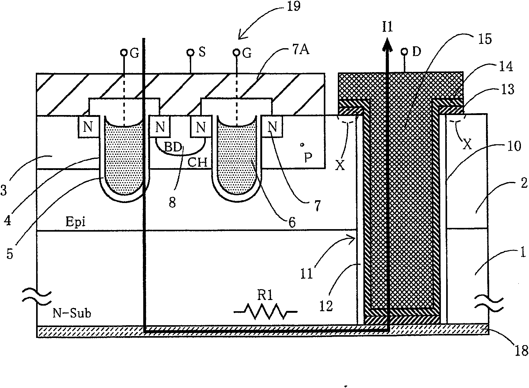
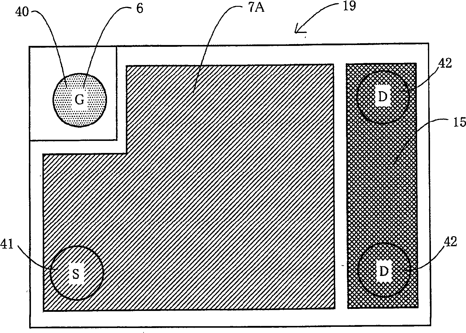
[0032] Here, the semiconductor device of the present invention will be described by taking an upper-drain type MOS transistor with a trench structure as an example.

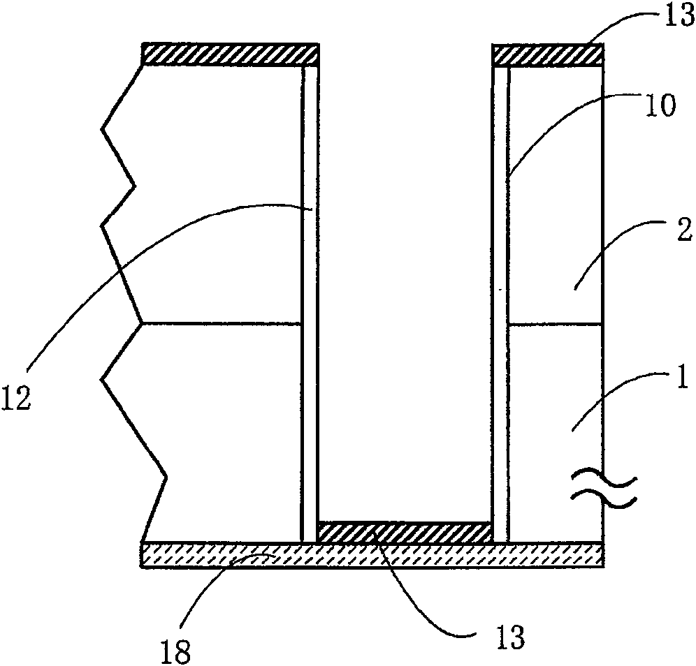
[0033] First, if figure 1 As shown, an N-type epitaxial layer 2 is formed on a semiconductor substrate 1 composed of one conductivity type such as N-type silicon, and a P-type diffusion layer 3 (channel region CH) is formed on the surface of the epitaxial layer 2 . In addition, in this embodiment, for example, the thickness of the epitaxial layer 2 is 10 μm, the thickness of the semiconductor substrate 1 including the thickness of the epitaxial layer 2 is 200 μm, and the thickness of the P-type diffusion layer 3 is 1 to 1.5 μm.

[0034] In addition, a groove 4 is formed at a predetermined depth from the P-type diffusion layer 3 to the above-mentioned epitaxial layer 2 . A conductive layer composed of a polysilicon film surrounded by an insulating film 5 is embedded in the trench 4 to form a gate electrode (G) 6...


PUM

PropertyMeasurementUnit
thicknessaaaaaaaaaa
thicknessaaaaaaaaaa
thicknessaaaaaaaaaa

Abstract

A semiconductor device for the purpose of achieving low resistance of the semiconductor device, characterized in that it has a through hole (10) formed on a semiconductor layer in contact with a first metal film (18); ) on the sidewall portion of the insulating film (12); formed on the first metal film (18) at the bottom of the through-hole (10) where the insulating film (12) is not formed and on the semiconductor layer The second metal film (13); the barrier metal film (14) formed on the insulating film (12) and the first metal film (18) in the through hole (10) and the barrier layer through the barrier layer A metal film (14) forms a wiring layer (15) in the through hole.

Description

technical field [0001] The present invention relates to a semiconductor device and a method of manufacturing the same, and more particularly, to a semiconductor device having a through electrode. Background technique [0002] A conventional semiconductor device will be described by taking a top-drain type MOS transistor with a trench structure as an example. [0003] That is, if Figure 14 As shown, for example, an epitaxial layer 52 is formed on a semiconductor substrate 51 composed of N-type silicon, and a P-type diffusion layer 53 (channel region CH) is formed on the surface layer of the epitaxial layer 52 . Further, a groove 54 is formed at a predetermined depth from the surface layer of the P-type diffusion layer 53 to the epitaxial layer 52 . A conductive layer composed of a polysilicon film surrounded by an insulating film 55 is embedded in the trench 54 to form a gate electrode (G) 56 . [0004] Furthermore, an N-type source layer 57 adjacent to the insulating film...

Claims


Application Information

Patent Timeline
Patent Type & Authority Patents(China)
IPC IPC(8): H01L29/417H01L21/28
Inventor 及川贵弘
Owner SANYO ELECTRIC CO LTD
Why Eureka
Try Eureka