Method for detecting silicon chip edge automatically

An automatic detection, silicon wafer technology, applied in the direction of semiconductor/solid-state device testing/measurement, etc., can solve the problems of inability to accurately locate the detection point, poor data analyzability, poor efficiency and accuracy, etc., to improve detection and monitoring efficiency, Improved analyzability, enhanced accuracy

Active Publication Date: 2010-02-17
SHANGHAI HUAHONG GRACE SEMICON MFG CORP
View PDF5 Cites 0 Cited by
  • Summary
  • Abstract
  • Description
  • Claims
  • Application Information

AI Technical Summary

Problems solved by technology

This kind of manual detection requires a lot of manpower and material resources, and the efficiency and accuracy are very poor. It is impossible to accurately locate the detection point, and the analyzability of the data is also poor.

Method used


Image

  • Method for detecting silicon chip edge automatically
  • Method for detecting silicon chip edge automatically
  • Method for detecting silicon chip edge automatically

Examples


Embodiment Construction

[0020] see figure 1 , the method for monitoring silicon chip edge of the present invention comprises the steps:

[0021] In the first step, the silicon wafer is scanned by an automatic defect detector, and the scanning result is saved as a file in KLARF format. When the automatic defect detector scans the silicon wafer, it can record the size and coordinates of each real defect on the silicon wafer.

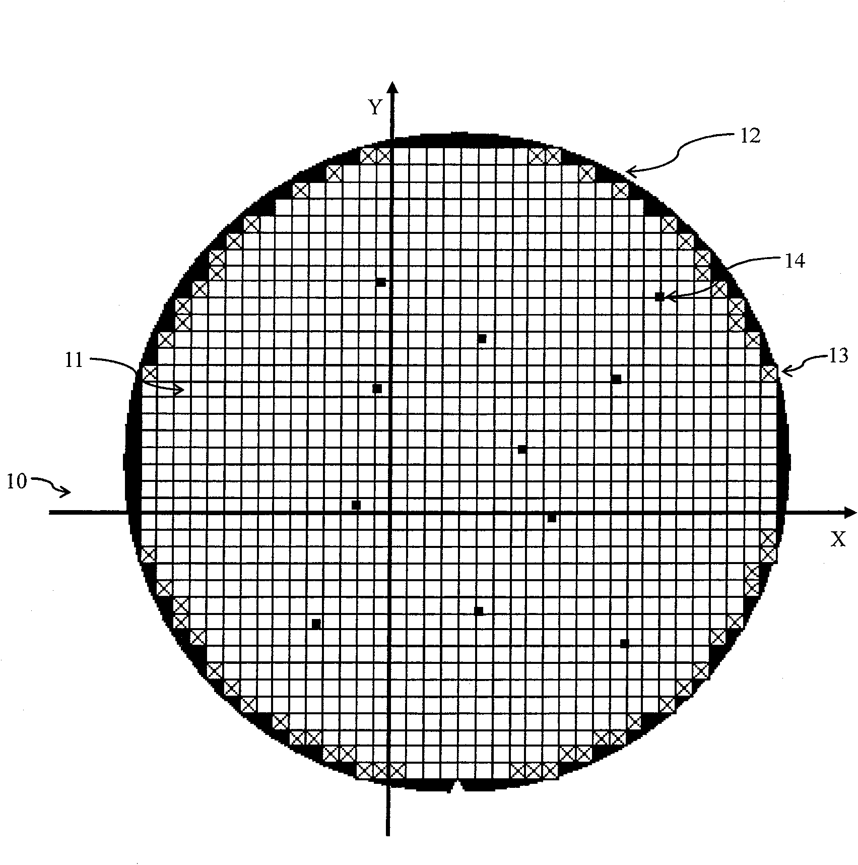
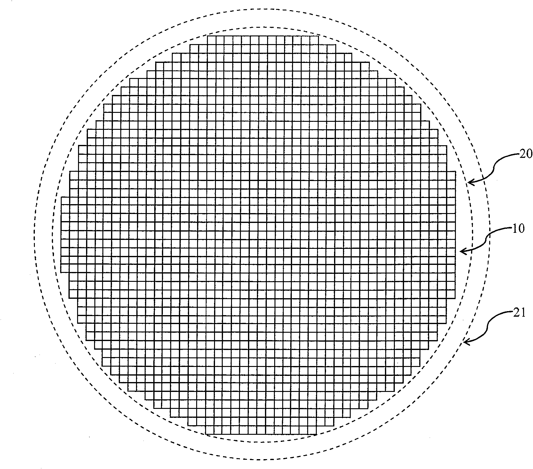
[0022] In the second step, a virtual wafer is added to the KLARF file saved in the first step, and the virtual wafer completely covers the edge of the entire silicon wafer. After the virtual wafer is added, the total area covered by the actual wafer and the virtual wafer of the KLARF file is larger than the actual area of ​​the silicon wafer.

[0023] The third step is to calculate the coordinates of the detection points on the edge of the silicon wafer in the coordinate system adopted by the KLARF file. The coordinate system used in the KLARF file is customized by the automat...


PUM


Abstract

The invention discloses a method for automatically detecting the edge of a silicon chip. The method comprises: step one, an automatic defect detector scans the silicon chip and stores a scanning result to form a file with a KLARF format; step two, a virtual crystal element is added to the KLARF file stored in the step one; the virtual crystal element integrally covers the edge of the whole siliconchip; step three, a coordinate of a detection point of the edge of the silicon chip is calculated in a coordinate system adopted by the KLARF file; step four, the coordinate of the detection point calculated in the step three is used as virtual defect and is added to the KLARF file edited in the step two; and step five, an electron scanning microscope is used to carry out automatic detection on the virtual defect of the KLARF file edited in the step four. Through functional integration of data analytic software and a detection machine, the method realizes automatic detection on the position of the edge of the silicon chip, saves manpower and material resource, improves efficiency and strengthens data accuracy and analyzability.

Description

technical field [0001] The invention relates to a semiconductor manufacturing process, in particular to a method for detecting defects on the edge of a silicon wafer Background technique [0002] At present, integrated circuit manufacturers detect the edge of patterned silicon wafers (that is, silicon wafers that have undergone certain processes such as etching processes on silicon wafers and have formed certain patterns such as etching patterns on silicon wafers) , is manually operated by a scanning electron microscope. [0003] In a production process, in which step is the defect on the edge of the silicon wafer produced, and how the existing defects on the edge of the silicon wafer evolve in the subsequent process? Perform multiple, repeated defect inspections on the wafer edge. This kind of manual detection requires a lot of manpower and material resources, and the efficiency and accuracy are very poor. It is impossible to accurately locate the detection point, and the...

Claims


Application Information

Patent Timeline
Patent Type & Authority Patents(China)
IPC IPC(8): H01L21/66
Inventor 王亚东
Owner SHANGHAI HUAHONG GRACE SEMICON MFG CORP
Why Eureka
Try Eureka