Ferroelectric field effect transistor storage device structure and preparation method

A technology of electric field effect and storage devices, which is applied in the fields of electric solid-state devices, semiconductor/solid-state device manufacturing, semiconductor devices, etc., can solve problems such as excessive working voltage, and achieve the effects of overcoming poor interface, good storage performance, and simple process

Inactive Publication Date: 2007-07-18
UNIV OF ELECTRONIC SCI & TECH OF CHINA
View PDF3 Cites 12 Cited by
  • Summary
  • Abstract
  • Description
  • Claims
  • Application Information

AI Technical Summary

Problems solved by technology

[0017] The patent utilizes MgO / SiO 2 Together they form a transition layer to form a ferroelectric field effect transistor with an MFIS structure. Due to the MgO / SiO 2 The voltage division effect of the layer will also lead to an excessively high operating voltage

Method used


Image

  • Ferroelectric field effect transistor storage device structure and preparation method

Examples


Embodiment Construction

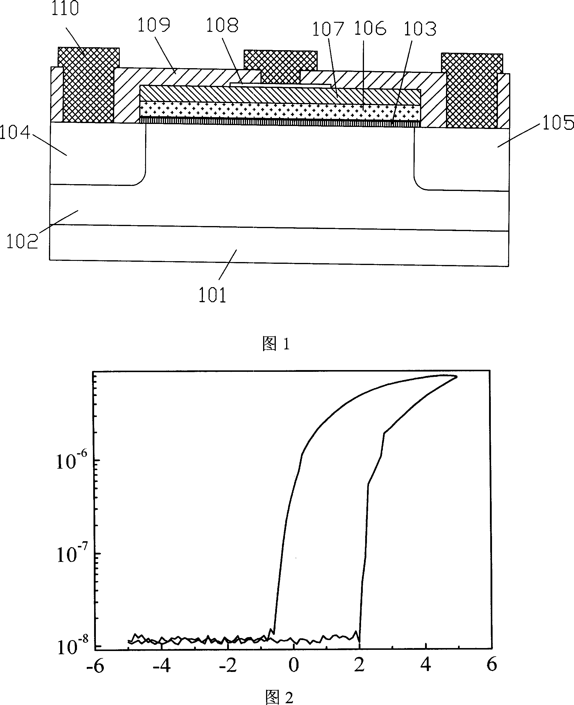
[0040] See Figure 1.

[0041] The ferroelectric field effect transistor of the present invention is composed of a substrate, a source region, a drain region and a gate region between the source region and the drain region, and the substrate is an n-type single crystal silicon wafer 101 with a (100) crystal orientation. After implantation to form the p-well 102, a layer of SiO is thermally oxidized on the surface 2 103 as an insulating layer.

[0042] The invention also includes directly forming p-channel transistors on n-type single-crystal silicon wafers.

[0043] Ferroelectric field effect transistor storage device structure, including Pt upper electrode 108, n + source region 104 and n + Drain region 105, layers from top to bottom are: PZT ferroelectric film 107, polysilicon 106, SiO 2 The insulating layer 103 , the p well 102 and the Si substrate 101 , and the upper electrode 108 are located on the PZT ferroelectric film 107 .

[0044] The preparation method of the a...


PUM


Abstract

The invention relates to a structure of ferroelectric memory and its preparation method, which specifically relates to a ferroelectric memory preparation technology of MFPIS structure. This invention includes: an upper electrode, a source region and a drain region. There are a PZT ferroelectric thin film, a multicrystal Si, an insulating layer, a well and a Si substrate, and the upper electrode lies on the PZT ferroelectric thin film. There are several beneficial effects of the invention, to overcome the general ferroelectric memory effect component contact surface difference, the working voltage high shortcoming, and have the good memory capability. This invention also provided the preparation method of this ferroelectric field effect transistor, and this preparation craft is simple, and compatible with the semiconductor manufacture craft.

Description

technical field [0001] The invention belongs to the field of microelectronic devices, and in particular relates to a preparation technology of a ferroelectric field effect transistor storage device with an MFPIS structure. Background technique [0002] Ferroelectric Field Effect Transistors (FFET) use a ferroelectric film as the gate dielectric layer in the transistor, and realize the modulation of the drain-source current through the gate polarization state, and read it according to the relative magnitude of the drain-source current A ferroelectric memory that stores information. The readout of the ferroelectric field effect transistor does not need to invert the gate polarization, and it is a non-destructive readout (NDRO) memory device. Compared with other non-volatile memories, FFET has the advantages of low operating voltage, high storage density, low power consumption and high read and write times, and has great application prospects in the field of information storag...

Claims


Application Information

Patent Timeline
IPC IPC(8): H01L29/78H01L27/115H01L21/336H01L21/8247
Inventor 蔡道林李平张树人
Owner UNIV OF ELECTRONIC SCI & TECH OF CHINA
Why Eureka
Try Eureka