Probe measurement device and system

A technology of probe measurement and probe head, applied in the field of probe measurement card, which can solve the problems of increased test cost, time-consuming and laborious, insufficient probe card area, etc.

Active Publication Date: 2007-07-25
POWERCHIP SEMICON MFG CORP
View PDF0 Cites 8 Cited by
  • Summary
  • Abstract
  • Description
  • Claims
  • Application Information

AI Technical Summary

Problems solved by technology

[0005] However, due to the current IC requirements of smaller size, stronger functions, and more pins, coupled with the successful development of the power signal sharing (Driver Share) test method, the test machine needs more probes , but the number of probes of the old probe card has not increased. If the traditional probe card is used for chip testing, it will not only be time-consuming and laborious, but also the

Method used


Image

  • Probe measurement device and system
  • Probe measurement device and system
  • Probe measurement device and system

Examples


Embodiment Construction

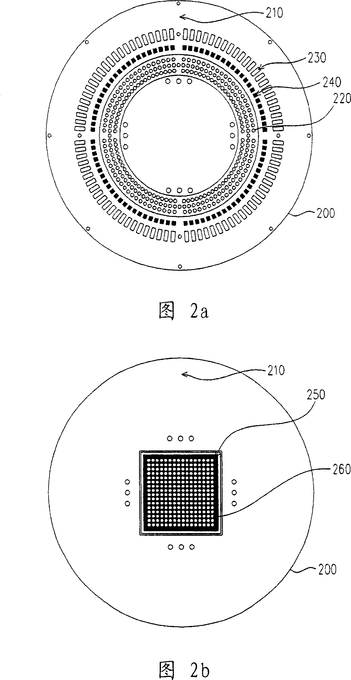
[0041] 2a and 2b are layout diagrams of a probe measuring device according to a preferred embodiment of the present invention. Please refer to Fig. 2a and 2b, this embodiment adopts the area that increases the circuit board of traditional probe card, changes the layout of each test element on the circuit board at the same time, and can increase the probe without changing the test motherboard. The number of probe heads on the card can be increased to achieve the purpose of improving test efficiency.

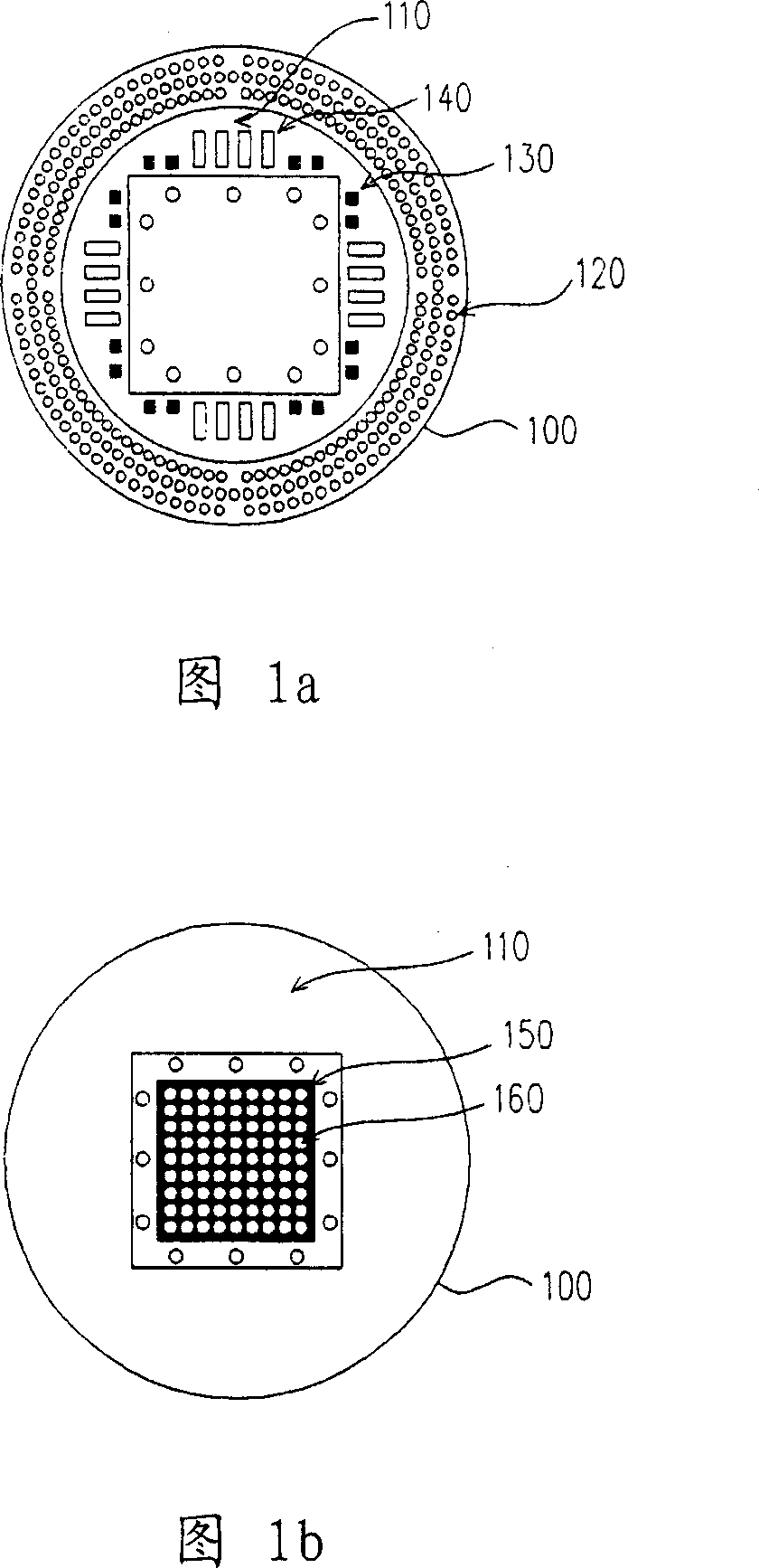
[0042] As shown in Figures 2a and 2b, the circuit board 210 of the probe measuring device 200 of this embodiment has been enlarged compared to the circuit board 110 of the existing probe card (as shown in Figures 1a and 1b), and is divided into upper and lower parts. Two sides, where Figure 2a shows the upper half and Figure 2b shows the lower half. In FIG. 2 a , a plurality of spring contacts 220 are disposed on the circuit board 210 , and these spring contacts 220 are arranged ...


PUM


Abstract

A probe measurement device is prepared for setting test elements larger circuit board and improving layout of test elements on circuit board for enabling to set more test elements on circuit board, furthermore enabling to arrange prepared measurement probe on old tester for raising probe measurement performance of old tester.

Description

technical field [0001] The invention relates to a wafer testing device, in particular to a probe measuring card which changes the layout of components to increase the number of configurable components. Background technique [0002] With the continuous evolution of semiconductor technology, the current transistor channel (Channel Length) has evolved from 0.15 microns to 0.13 microns, and further developed to the latest 90-nanometer process. In the semiconductor process, before the wafer process is completed and the packaging is not cut, in order to ensure the yield of the wafer and avoid the waste of the packaging, the electrical and functional tests at the wafer stage must be carried out first. This test method is to use the test machine and the probe card (Probe Card) to form a test circuit, and directly connect the probe head (Probe Pin) on the probe card to the pad (Pad) or bump (Bump) on the chip Contact, and use the probe to detect each chip on the wafer, so as to lead...

Claims


Application Information

Patent Timeline
IPC IPC(8): G01R1/073G01R1/067G01R31/26H01L21/66
Inventor 许繁贤
Owner POWERCHIP SEMICON MFG CORP
Why Eureka
Try Eureka