Dual field plate mesfet and its forming method

A field-effect transistor and metal-semiconductor technology, applied in the field of metal-semiconductor field-effect transistors, can solve problems such as channel burnout, limiting MESFET high-voltage operating characteristics, limiting MESFET operating range and robustness, etc.

Inactive Publication Date: 2007-07-25
COBHAM DEFENSE ELECTRONICS SYST CORP
View PDF0 Cites 5 Cited by
  • Summary
  • Abstract
  • Description
  • Claims
  • Application Information

AI Technical Summary

Problems solved by technology

However, the gate field plate does not affect the high field region in the drain ohmic contact region which also causes channel burnout
The burnout potential close to the drain contact limits the operating range and robustness of MESFETs for high voltage applications
Thus, the gate Schottky and / or drain contact area limits the high voltage operating characteristics of the MESFET

Method used


Image

  • Dual field plate mesfet and its forming method
  • Dual field plate mesfet and its forming method
  • Dual field plate mesfet and its forming method

Examples


Embodiment Construction

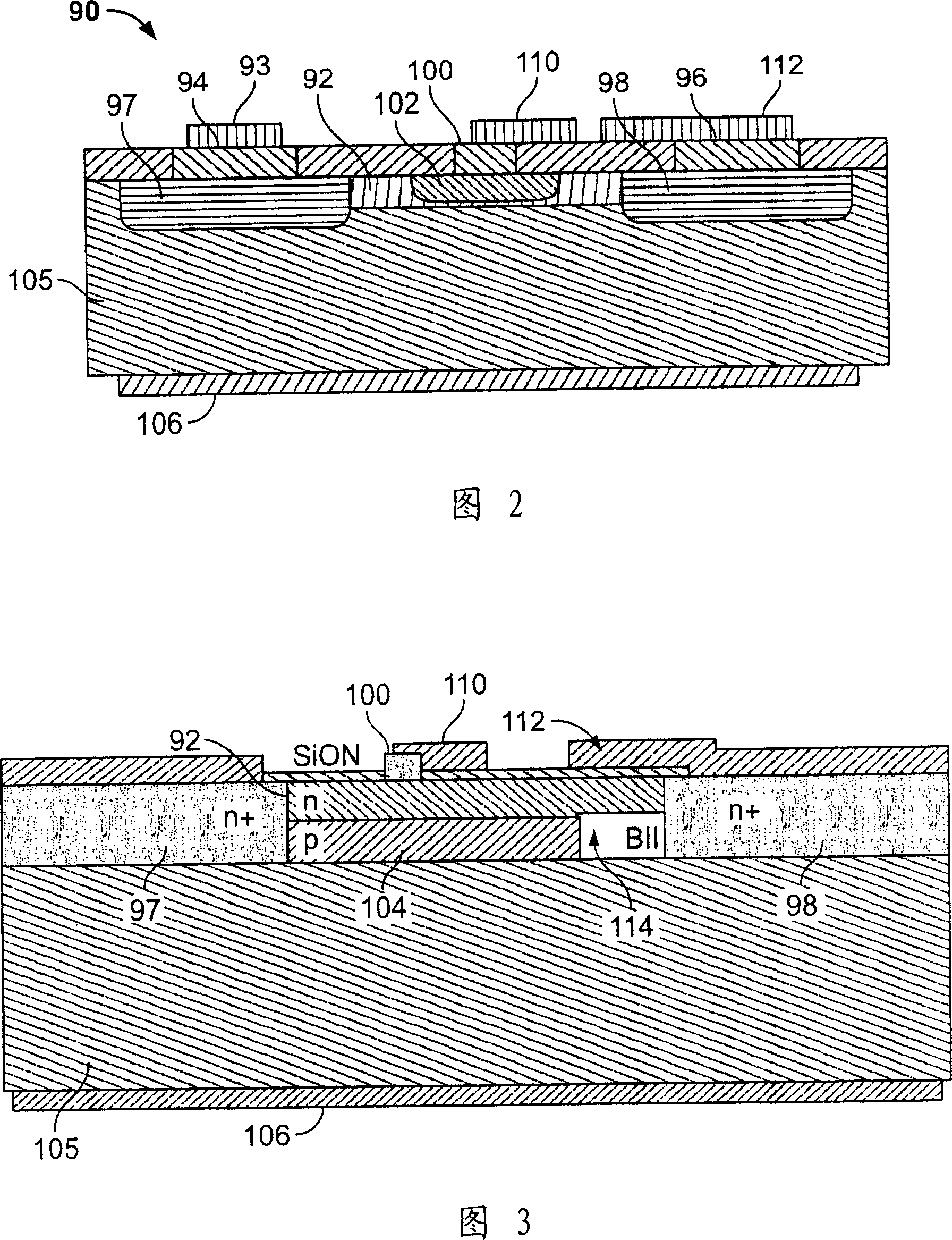
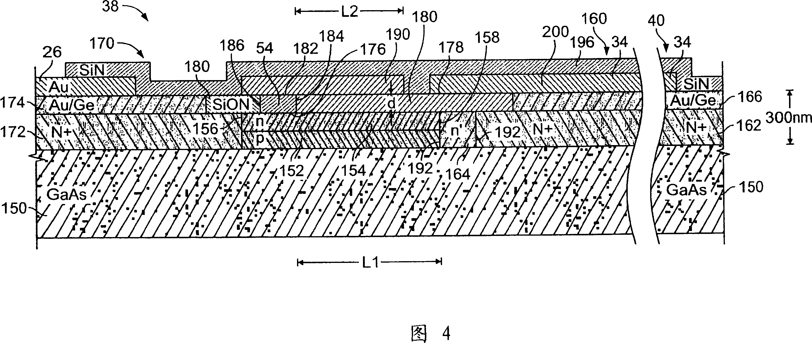
[0015] Various embodiments of the present invention provide a metal semiconductor field effect transistor (MESFET) with a drain side field plate. More specifically, in addition to the gate Schottky and the gate-side field plate extending toward the drain contact, various embodiments of the MESFET include a drain-side field plate extending toward the gate contact. The formation of the drain side field plate may be provided simultaneously with the formation of the gate field plate.

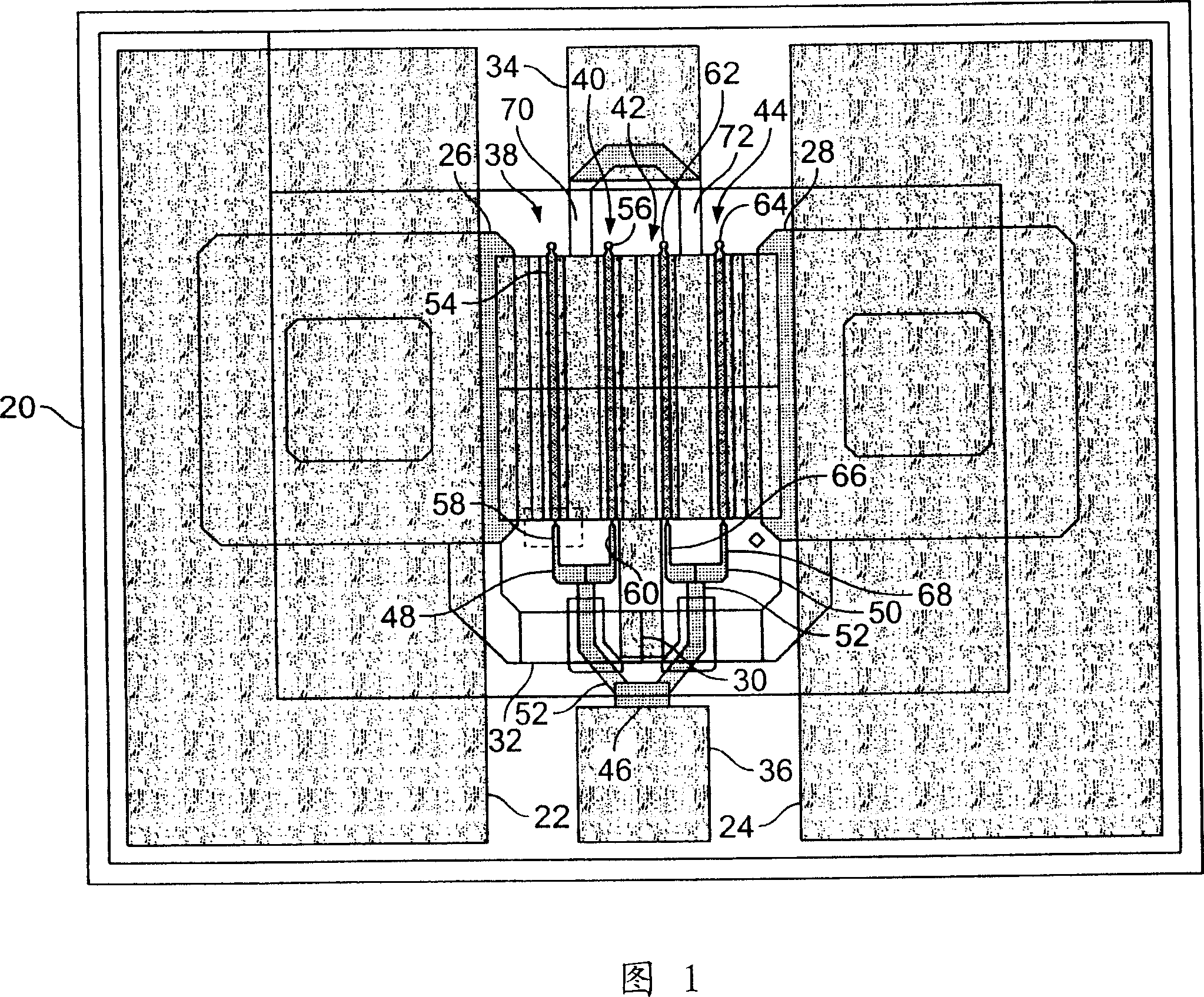
[0016] Generally, as shown in FIG. 1 , one or more MESFETs formed in accordance with various embodiments of the present invention are formed on a die 20 . More specifically, first ground plane 22 and second ground plane 24 include metal or metallization portions 26 , 28 , and 30 that define conductors or electrodes that are electrically coupled in parallel through conductive paths 32 . A drain electrode 34 configured as a contact or solder pad and a gate electrode 36 which may also be configured as...


PUM


Abstract

A dual field plate MESFET (90) and method of forming a MESFET. The MESFET (90) includes a gate electrode (100) and a drain electrode (96), with the gate electrode (100) and drain electrode (96) formed on a substrate (105). The MESFET further includes a gate side field plate (110) at the gate electrode (100) and a drain side field plate (112) in proximity to the drain electrode (96) and extending over a burnout improvement region in the substrate (105).

Description

technical field [0001] The present invention relates generally to semiconductor devices, and more particularly to metal semiconductor field effect transistors (MESFETs). Background technique [0002] MESFETs, also known as Schottky gate field effect transistors (FETs), such as GaAs MESFETs, can be used in many different electronic applications. These applications range from providing switching operations (eg, high-speed digital switching) to providing signal amplification. Additionally, these applications include commercial, industrial and military applications. [0003] MESFETs are often included in devices used in microwave frequency communications and radar. This device and other devices and systems using or incorporating MESFETs have ever-increasing power requirements. For example, the desired power output per MESFET device, such as per transistor surface area, continues to increase. Since the power output of transistors operating at high voltages is also greatly imp...

Claims


Application Information

Patent Timeline
Patent Type & Authority Applications(China)
IPC IPC(8): H01L29/812H01L29/417H01L21/338H01L21/28
CPCH01L29/812H01L29/404
Inventor 托马斯·A·温斯洛
Owner COBHAM DEFENSE ELECTRONICS SYST CORP
Why Eureka
Try Eureka