Flash memory system compensating reduction in read margin between memory cell program states
一种存储系统、存储单元阵列的技术,应用在信息存储、静态存储器、只读存储器等方向,能够解决难以保证状态读余量、难以知道存储单元状态、阈值电压降低等问题
- Summary
- Abstract
- Description
- Claims
- Application Information
AI Technical Summary
Problems solved by technology
Method used
Image

Examples
Embodiment Construction
[0022] Now, the present invention will be described more fully hereinafter with reference to the accompanying drawings, in which preferred embodiments of the invention are shown. This invention may, however, be embodied in many different forms and should not be construed as limited to the embodiments set forth herein. Rather, these embodiments are provided so that this disclosure will be thorough and complete, and will fully convey the scope of the invention to those skilled in the art. Like reference numerals refer to like elements throughout the figures.
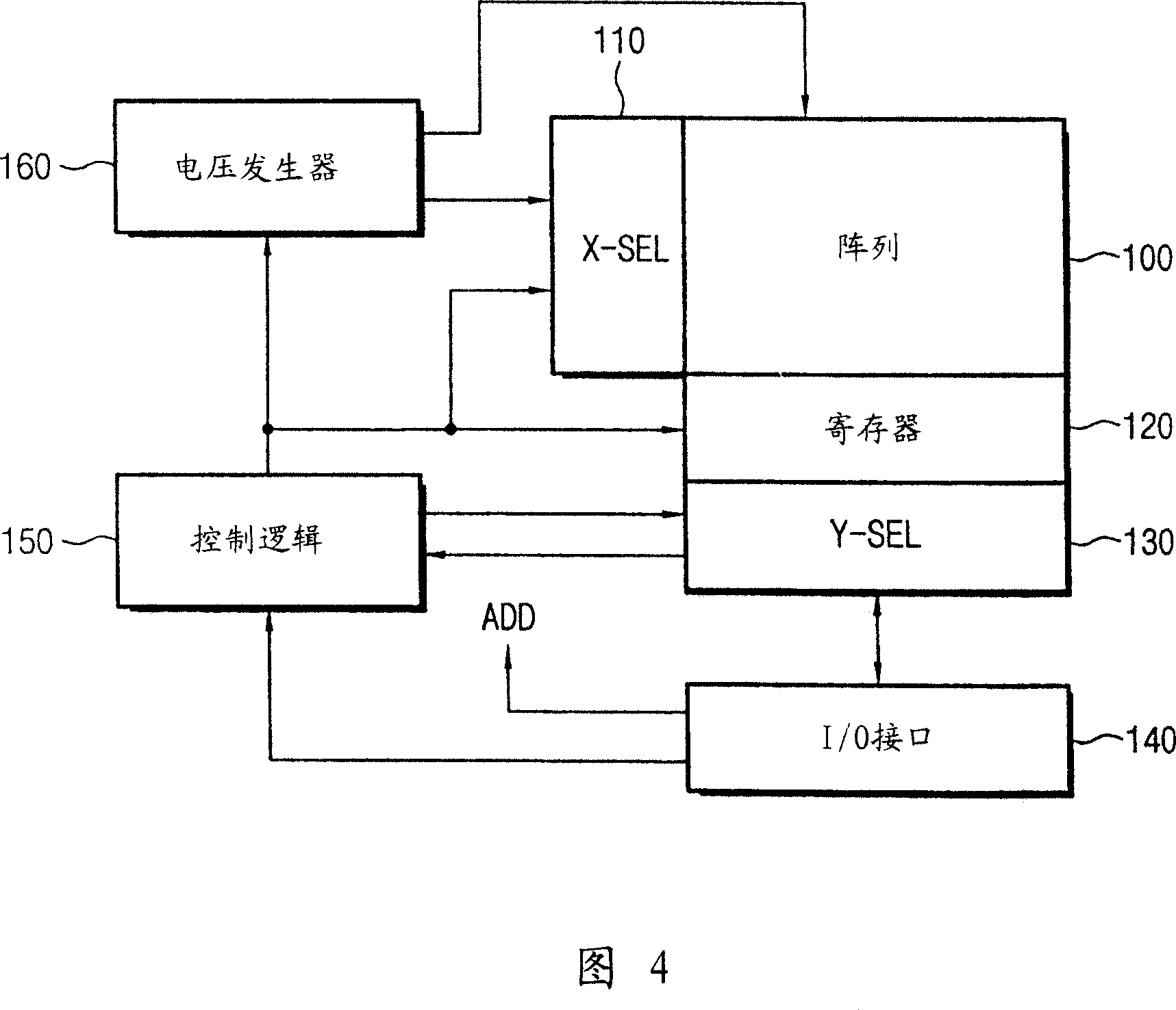
[0023] FIG. 4 is a block diagram of a flash memory device according to an embodiment of the present invention, which includes a memory cell array 100 for storing data information. The memory cell array 100 includes a plurality of memory blocks each having the memory cell configuration shown in FIG. 5 .
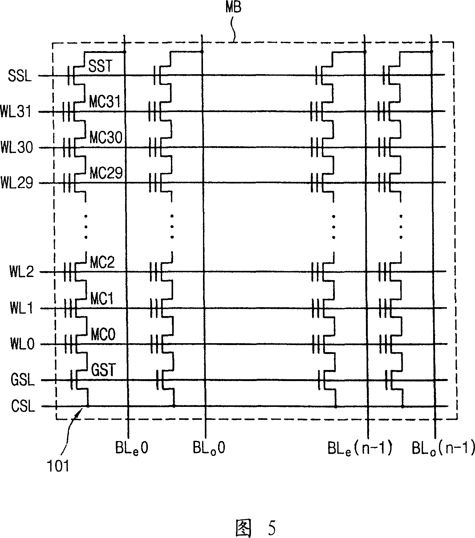
[0024] 5 is a circuit diagram of the memory cell array shown in FIG. 4, which includes a memory block MB containing a ...
PUM
 Abstract
Description
Claims
Application Information
 - Generate Ideas
- Intellectual Property
- Life Sciences
- Materials
- Tech Scout
- Unparalleled Data Quality
- Higher Quality Content
- 60% Fewer Hallucinations
Browse by: Latest US Patents, China's latest patents, Technical Efficacy Thesaurus, Application Domain, Technology Topic, Popular Technical Reports.
© 2025 PatSnap. All rights reserved.Legal|Privacy policy|Modern Slavery Act Transparency Statement|Sitemap|About US| Contact US: help@patsnap.com