

Mask film formation method and mask film formation apparatus
A film forming method and mask technology, applied in microlithography exposure equipment, vehicle design optimization, instruments, etc., can solve problems such as controlling the temperature of substrates and masks
- Summary
- Abstract
- Description
- Claims
- Application Information
AI Technical Summary
Problems solved by technology
Method used
Image

Examples
example 1
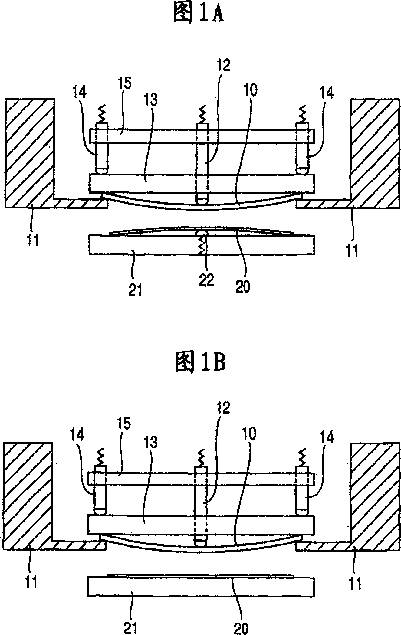
[0050] Mask film formation was performed using the apparatus of FIG. 1A.
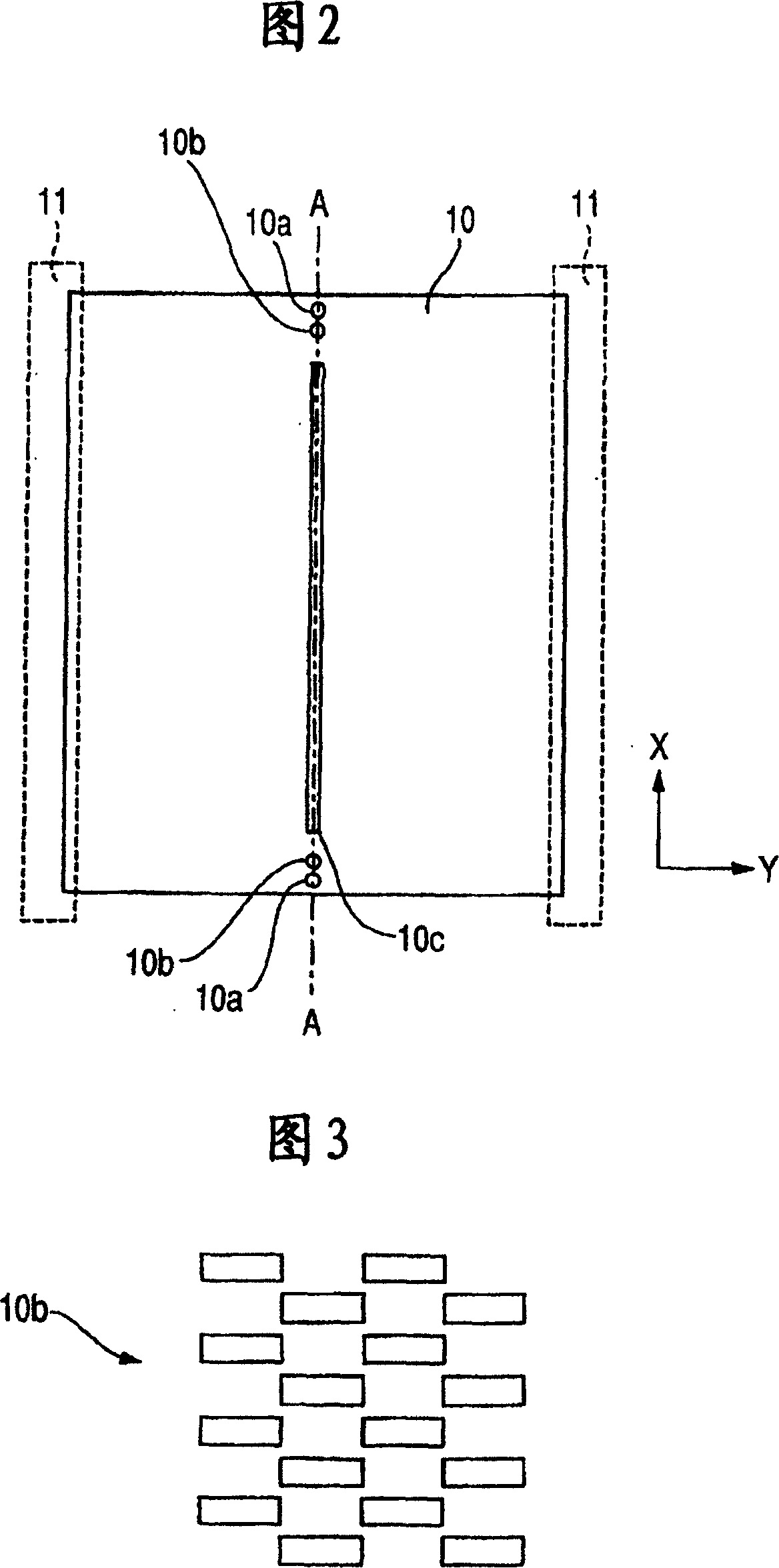
[0051] For the substrate 10 , an alkali-free glass having an area of 400 mm×500 mm and a thickness of 0.6 mm was used. In the substrate 10, a Cr electrode formed into a pattern by a photolithography step and an alignment mark 10b formed as shown in FIG. 3 are disposed. The formed Cr electrode pattern had a size of 50 μm×150 μm.
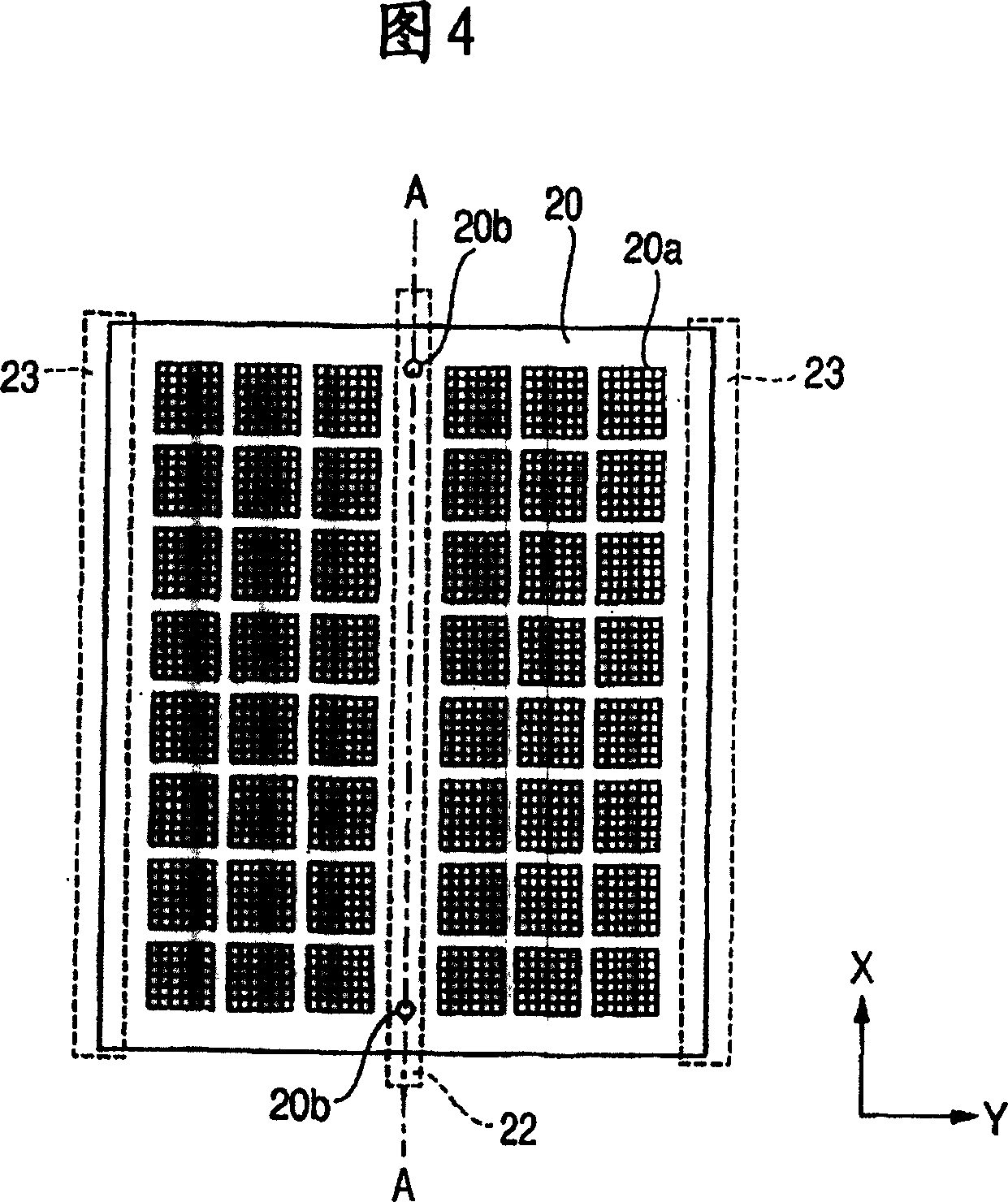
[0052] For the mask 20 , a thin film mask having an area of 430 mm×530 mm and a thickness of 50 μm was formed according to the electroforming method and used. For the material of the mask 20, Ni was used. An alignment mark 20 b having the same position and size as the alignment mark 10 b made of a Cr electrode of the substrate 10 is formed in the mask 20 . The alignment mark 20b of the mask 20 is formed simultaneously with the step of forming the mask pattern (opening) 20a shown in FIG. 4 .
[0053] The test was carried out using the apparatus shown in Figs. 1A and 1B i...
example 2
[0061] According to the same procedure as in Example 1, a state was formed in which, on the mask holder 21 held horizontally, the mask 20 and the substrate 10 were held horizontally and closely adhered to each other.
[0062] In addition, the planar member 13 behind the substrate is brought into abutment against the rear side of the substrate, and after the electromagnet behind the planar member 13 is brought into abutment on the planar member 13, the electromagnet applies electromagnetic force to the mask. In this case, until the electromagnetic force of the electromagnet is applied, the pressing force of the substrate pressing member 12 is maintained. In addition, the mask holder 21 is gradually moved vertically so that the mask 20, the substrate 10, the planar member 13 and the electromagnet are combined into an unbent state.
[0063] In this state, the measurement shows that the amount of positional deviation between the substrate 10 and the mask 20 is within a practical t...
example 3
[0065] According to the same procedure as in Example 2, the mask 20, the substrate 10, the planar member 13, and the electromagnet were combined to form a non-bent state. This mechanism provides a coolant path within the planar member 13, and continuously supplies cooling water whose temperature is controlled at 23°C.
[0066] In this state, a deposition source (not shown) provided 300 mm below the mask 20 was heated to deposit a deposition material (Alq3: manufactured by Dojin Chemistry) on the substrate 10 via the mask 20 . In this case, at the opening, the temperature of the deposition source was 315°C.
[0067] 100 consecutive trials were carried out for deposition. After deposition, the substrate 10 was removed from the vacuum; measurements showed that the amount of positional misalignment between the film patterned on the substrate surface (on the Cr electrodes) and the Cr electrodes on the substrate 10 was within practical tolerances across the substrate Within, that ...
PUM
 Abstract
Description
Claims
Application Information