Stacked chip package using warp-proof insulative material and method of manufacturing the same

A technology of insulating layer and substrate material, which is applied in semiconductor/solid-state device manufacturing, auxiliary products for massage, and equipment for compressing reflection points, etc. It can solve problems such as fracture and peeling, and affect the reliability of yield devices

Inactive Publication Date: 2007-08-29
SAMSUNG ELECTRONICS CO LTD
View PDF2 Cites 16 Cited by
  • Summary
  • Abstract
  • Description
  • Claims
  • Application Information

AI Technical Summary

Problems solved by technology

When subjected to extensive heating and cooling thermal cycles, this CTE mismatch can cause more cracki

Method used


Image

  • Stacked chip package using warp-proof insulative material and method of manufacturing the same
  • Stacked chip package using warp-proof insulative material and method of manufacturing the same
  • Stacked chip package using warp-proof insulative material and method of manufacturing the same

Examples


Embodiment Construction

[0070]The present invention will now be described more fully with reference to the accompanying drawings, in which preferred embodiments of the invention are shown. This invention may, however, be embodied in different forms and should not be construed as limited to the example embodiments set forth herein. In the drawings and related descriptions, if a first layer is referred to as being "on" another layer, the first layer can be directly on the other layer, or intervening layers may be present. Like numbers refer to like elements throughout the specification.

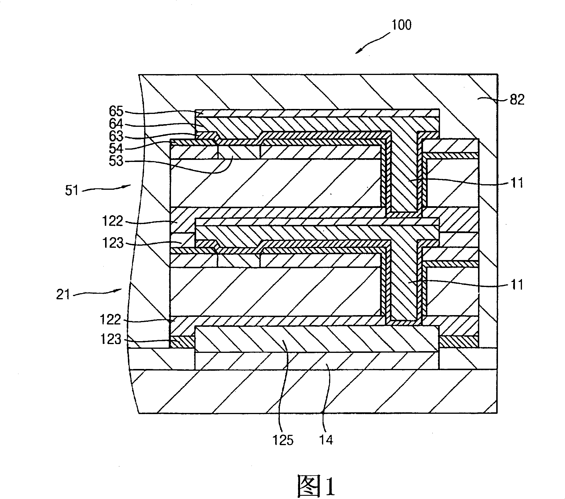
[0071] FIG. 1 is a cross-sectional view of a stacked die package according to the present invention. The stacked chip package according to the embodiment of FIG. 1 includes a printed circuit board 10 on which a chip stack including a first chip 21 and a second chip 51 is mounted. Each of the first and second chips 21, 51 includes a plurality of bond pads 53 for exchanging signals with locations off the chip and cond...


PUM


Abstract

In laminated chip structure and manufacturing method thereof, relative simple technology is used for fully filling the clearance between upper chip and lower chip thereby eliminating the clearance and preventing problems of fracture and stripping in relation of the clearance. The invention can be used in bonding method of chip level and wafer level. Before laminating chips or wafers, photosensitive polymer layer is applied on a first chip or wafer. The photosensitive polymer layer is partly solidified in order to stabilize structure thereof and keep adhesiveness performance thereof. A second chip or wafer is laminated, aligned and bonded to the first chip or wafer, and then the photosensitive polymer layer is solidified to completely bond the first and the second chips or wafers. In this manner, the adhesiveness between chips/wafers is greatly improved as well as clearance is fully filled. In addition, mechanical reliability is improved and mismatch of CTE is reduced, and warpage, fracture and stripping related problems can be reduced, thus, the rate of finished products and reliability can be improved.

Description

[0001] related application [0002] This application claims priority under 35 U.S.C. 119 to Korean Patent Application No. 10-2006-0007109 filed on Jan. 24, 2006, the contents of which are incorporated herein by reference in their entirety. This application is related to U.S. Patent Application Serial No. 11 / 436,851 to Yong-Chai Kwon et al., entitled "Stacked Chip Package Using Photosensitive Polymer and Manufacturing Method Thereof," which was filed on the same date as this application and of the same owner, the contents of which are hereby incorporated by reference in their entirety. technical field [0003] The present invention relates to a semiconductor device package including a stacked chip package structure using a photosensitive polymer including tape tack and anti-warping properties, and a method of manufacturing the same. Background technique [0004] Semiconductor manufacturing and packaging technologies have advanced to the point where a device package may incl...

Claims


Application Information

Patent Timeline
IPC IPC(8): H01L21/50H01L21/56H01L21/60H01L25/00H01L25/065H01L23/29H01L23/488
CPCH01L2224/16145A61H39/04A61H7/003A61H2205/065A61H2201/1253
Inventor 权容载李康旭马金希韩成一李东镐
Owner SAMSUNG ELECTRONICS CO LTD
Why Eureka
Try Eureka