

Organic electroluminescent device
An electroluminescent device, organic technology, applied in the direction of electroluminescent light source, electric solid device, electric light source, etc., can solve the problems affecting the spectral characteristics of the device, achieve the effect of improving luminous efficiency, ensuring color purity, and improving composite efficiency
- Summary
- Abstract
- Description
- Claims
- Application Information
AI Technical Summary
Problems solved by technology
Method used
Image

Examples
Example Embodiment
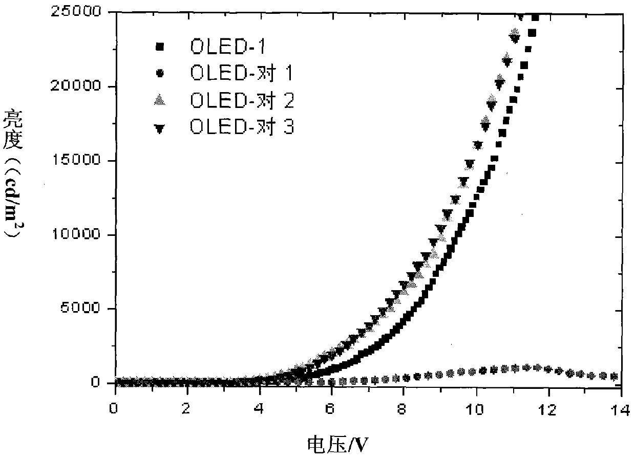
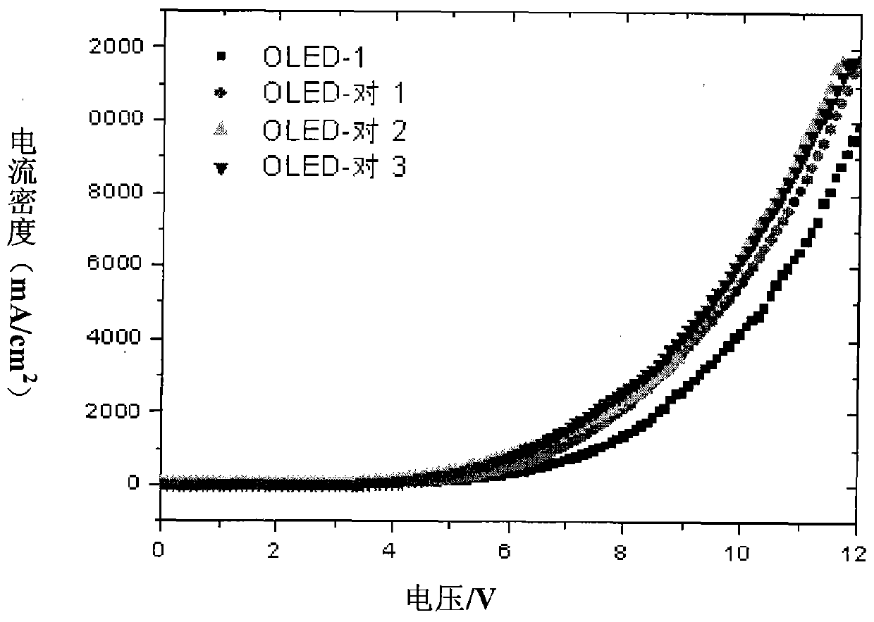
Embodiment 1: (part number OLED-1)
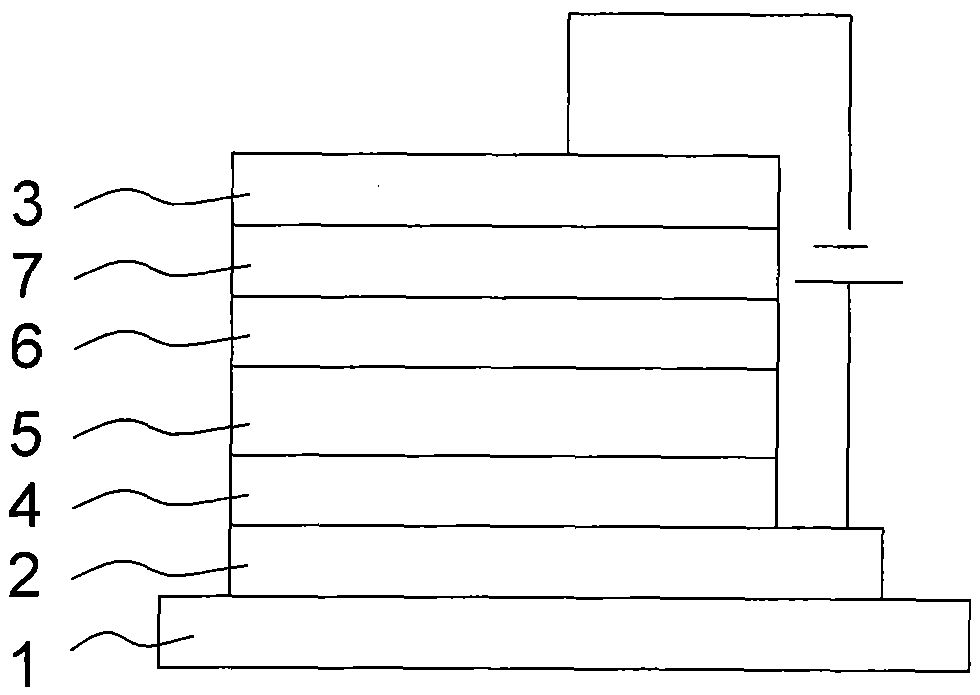
Glass / ITO / NPB / NPB: BiF 3 / NPB / Alq 3 / LiF / Al (1)
The specific preparation method of the organic electroluminescent device with the above structural formula (1) is as follows:
① Clean the glass substrate by ultrasonic method of boiling detergent and deionized water, place it under an infrared lamp and dry it, and vapor-deposit a layer of anode material on the glass with a film thickness of 180nm;
②Place the above-mentioned glass substrate with anode in a vacuum chamber, and evacuate to 1×10 -5 Pa, continue to vapor-deposit the hole transport layer on the above-mentioned anode layer film, first vapor-deposit a layer of NPB film, the rate is 0.1nm / s, and the thickness of the vapor-deposited film is 20nm; and BiF 3 The evaporation rate ratio is 1:1, BiF 3The doping concentration in NPB is 50wt%, the total evaporation rate is 0.1nm / s, and the evaporation film thickness is 10nm; then a layer of NPB thin film is evaporated, the rate is 0.1nm...
Example Embodiment
Example 2
Glass / ITO / HIL / NPB: BiF 3 (x%) / NPB / Alq 3 / LiF / Al (5)
The specific preparation method of the organic electroluminescent device with the above structural formula (5) is as follows:
① Clean the glass substrate by ultrasonic method of boiling detergent and deionized water, and dry it under an infrared lamp, and vapor-deposit a layer of anode material on the glass with a film thickness of 150nm;
② Put the above-mentioned glass substrate with the anode layer in the vacuum chamber, and evacuate to 1×10 -5 Pa, continue to vapor-deposit a layer of hole injection layer on the above-mentioned anode layer film, the vapor-deposited film thickness is 100nm, and then vapor-deposit the hole transport layer. 3 The evaporation rate ratio of 1:x, BiF 3 The doping concentration in NPB is x wt%, the total evaporation rate is 0.2nm / s, and the film thickness is 15nm; continue to evaporate a layer of NPB film, the evaporation rate is 0.1nm / s, and the film thickness is 20nm; In this ...
Example Embodiment
Example 3
Glass / ITO / NPB / NPB: BiF 3 (x%) / NPB / Alq / LiF / Al (6)
The specific preparation method of the organic electroluminescent device with the above structural formula (6) is as follows:
Steps ①, ③ and ④ are the same as in Example 1. In step ②, a layer of NPB is evaporated on the anode layer with a film thickness of 20nm, and then double-source co-evaporation is used for doping. NPB and BiF 3 The evaporation rate is 1:x, BiF 3 The doping concentration in NPB is x wt%, the total evaporation rate is 0.2nm / s, and the film thickness is 10nm; continue to evaporate a layer of NPB thin film, the evaporation rate is 0.1nm / s, and the film thickness is 20nm.
The device structure performance data of different doping concentrations are shown in Table 3 below, and the corresponding device performance diagram is shown in Figure 4:
Table 3 Device structure of doped part x wt% Driving voltage (V, @200nit) Current density (A / m 2 , 6V) Luminous Efficiency (cd / A, @200nit) NPB(50nm) 0 4.5...
PUM
 Abstract
Description
Claims
Application Information