Image display device
An image display and device technology, applied in image/graphic display tubes, electrical components, cold cathodes of discharge tubes, etc., can solve the problems of low brightness and insufficient anode power supply, and achieve the effect of large selection of materials and preventing voltage reduction.
- Summary
- Abstract
- Description
- Claims
- Application Information
AI Technical Summary
Problems solved by technology
Method used
Image

Examples
Embodiment 1
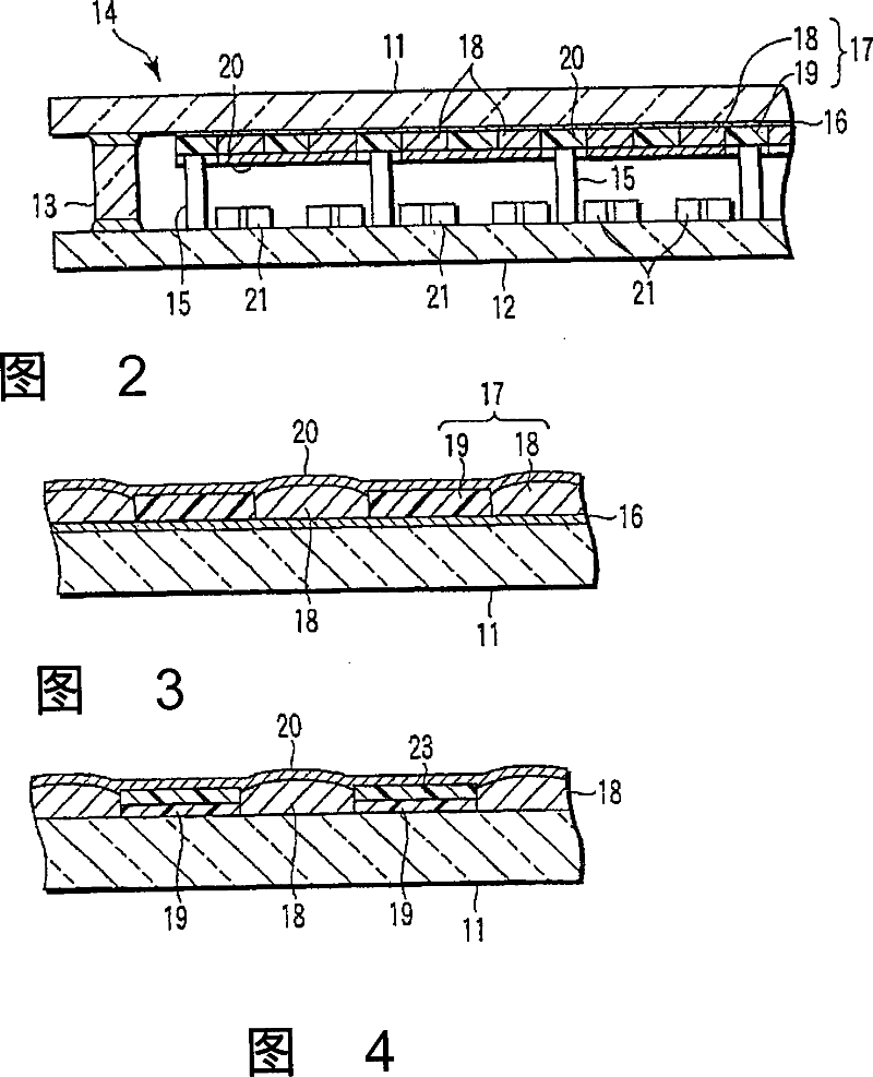
[0042] The image display device of Example 1 is shown in FIG. 3 . On the inner surface of the front plate 11 made of glass, a fluorescent surface 17 is formed through an ITO transparent electron conducting film (200 nm thick) 16 functioning as an anode feeder wiring. An anode power supply terminal (not shown) connected to the transparent electronically conductive film 16 is connected to the inner surface of the front plate 11 . The phosphor surface 17 has a phosphor layer 18 formed on the front plate 11 that respectively emits red (R), green (G), and blue (B) light, and at least a part of which also serves as a resistive material layer arranged in a matrix. A light absorbing layer (shading layer) 19 with a thickness of 10 μm. Here, the resistance value of the light-shielding layer 19 that doubles as a resistive material layer is set to about 1×10 4 Europe. A metal back layer 20 made of aluminum (Al) with a thickness of 80 nm is formed in a rectangular shape on the fluoresce...
Embodiment 2
[0045] The image display device of embodiment 2 constitutes as shown in Figure 4, gets at least a part to double as the thick 5 micron light-shielding layer 19 of anode power supply wiring, and forms the thick 10 micron resistance material layer (resistance value is about 1 * 10 4 Europe) 23, so that it covers the light-shielding layer 19. Furthermore, an anode power supply terminal (not shown) connected to the light-shielding layer 19 serving also as the anode power supply wiring is connected to the inner surface of the front plate 11 . The light-shielding layer 19 and the metal backing layer 20 are arranged to face each other with the resistive material layer 19 interposed therebetween.
[0046] According to Example 2, the same effect as that of Example 1 is obtained.
Embodiment 3
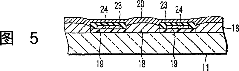
[0048] The structure of the image display device of Example 3 is shown in FIG. 5 . On at least a part of the light-shielding layer 19, an anode power supply wiring 24 with a thickness of 5 micrometers is stacked, and the resistance value is about 1×10. 4 The resistive material layer 23 is 10 micrometers thick so as to surround the anode power supply wiring 24 . An anode power supply terminal (not shown) connected to the anode power supply wiring 24 is connected to the inner surface of the front plate 11 . The anode power supply wiring 24 and the metal backing layer 20 are arranged to face each other with the resistive material layer 23 interposed therebetween.
[0049] According to Example 3, the same effect as that of Example 1 is obtained.
PUM
 Abstract
Description
Claims
Application Information
 - R&D
- Intellectual Property
- Life Sciences
- Materials
- Tech Scout
- Unparalleled Data Quality
- Higher Quality Content
- 60% Fewer Hallucinations
Browse by: Latest US Patents, China's latest patents, Technical Efficacy Thesaurus, Application Domain, Technology Topic, Popular Technical Reports.
© 2025 PatSnap. All rights reserved.Legal|Privacy policy|Modern Slavery Act Transparency Statement|Sitemap|About US| Contact US: help@patsnap.com