Check patentability & draft patents in minutes with Patsnap Eureka AI!

Gamma reference voltage generation circuit

A reference voltage and circuit generation technology, which is applied in nonlinear optics, instruments, optics, etc., can solve the problems of display resolution limitation, affecting the work efficiency of engineers and technicians, and cumbersome gamma resistance value, so as to improve the accuracy of the circuit and reduce the Area and power consumption, the effect of simple circuit

Active Publication Date: 2007-10-31
BEIJING BOE OPTOELECTRONCIS TECH CO LTD +1
View PDF0 Cites 19 Cited by
  • Summary
  • Abstract
  • Description
  • Claims
  • Application Information

AI Technical Summary

Problems solved by technology

[0006] The main disadvantage of the prior art is that the determination of the gamma resistance value is very cumbersome, and different TFT liquid crystal display panels and different liquid crystal material characteristics need to be adjusted with different gamma resistance values, so a large amount of calculation and debugging work is required , greatly affecting the work efficiency of engineers and technicians
Moreover, each gamma reference voltage value should be input to the pins of the corresponding signal drive circuit, and often in order to improve the grayscale display characteristics, the number of gamma reference voltages will be increased, and the prior art needs to increase the corresponding number of signal drive circuits. Circuit input pins, so it is not conducive to the integration of signal drive circuits, which limits the display resolution

Method used


Image

  • Gamma reference voltage generation circuit
  • Gamma reference voltage generation circuit
  • Gamma reference voltage generation circuit

Examples


Embodiment Construction

[0019] The present invention will be further described in detail below in conjunction with the accompanying drawings and specific embodiments.

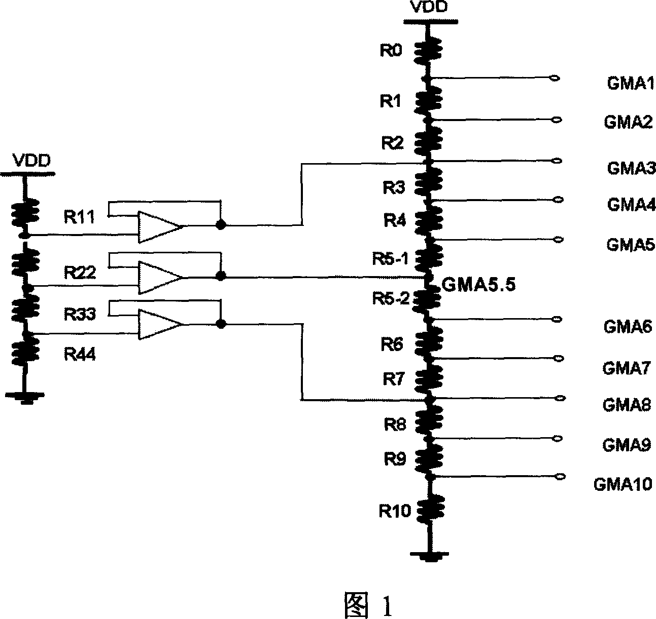
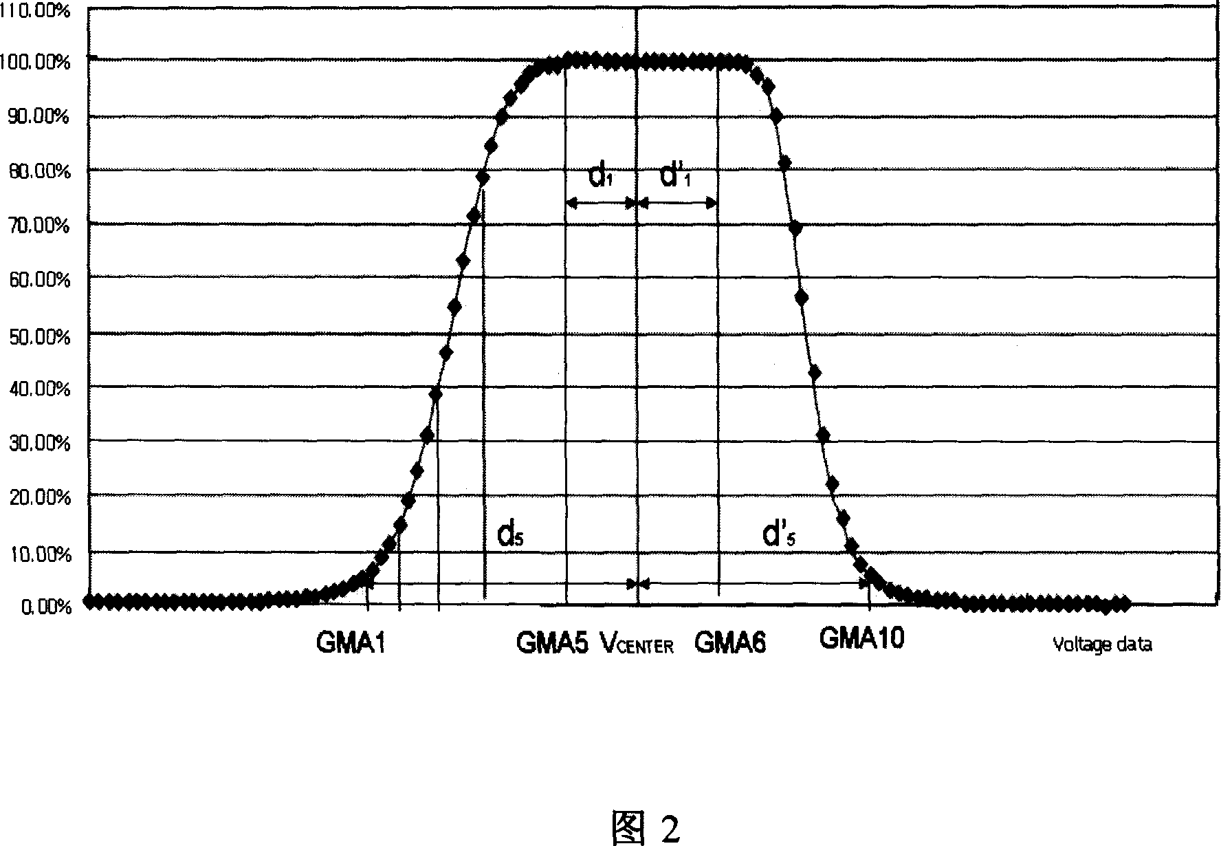
[0020] A liquid crystal material used in a thin film transistor liquid crystal display has a symmetrical voltage-transmittance characteristic curve as shown in FIG. 2 . Each gamma reference voltage value is determined according to the characteristic curve and the required gray scale. If it is determined that the gamma reference voltage values ​​in the positive pressure area are GMA1, GMA2, GMA3, GMA4, and GMA5, then due to the symmetrical voltage-transmittance characteristic curve, the gamma reference voltage values ​​​​in the negative pressure area GMA6, GMA7, GMA8, GMA9 , GMA10 and the gamma reference voltage values ​​GMA1 , GMA2 , GMA3 , GMA4 , GMA5 in the positive pressure zone are mirror images of each other with respect to the symmetrical center voltage VCNETER of the voltage-transmittance characteristic curve. which is:

[00...


PUM


Abstract

This invention discloses one Gamma reference voltage generation circuit for film transistor LCD, which comprises direct stable voltage, positive gamma reference voltage generation circuit and is characterized by the following: the said reference voltage generate circuit output end is connected with switch and reverse charge pump circuit to form negative Gamma reference generation circuit; according to LCD symmetric voltage to transparence property curve by simple circuit and positive Gamma reference voltage to Gamma reference voltage.

Description

technical field [0001] The invention relates to a thin film transistor liquid crystal display (TFT-LCD), in particular to a gamma (GAMMA) reference voltage generating circuit of the thin film transistor liquid crystal display. Background technique [0002] Liquid crystal display technology is developing very fast, and due to its light weight, liquid crystal display devices are widely used in various display fields. [0003] As an important part of the TFT-LCD module, the gamma reference voltage generation circuit plays a vital role in the gray scale adjustment of the TFT-LCD. The function of the gamma reference voltage generation circuit is to set the gamma reference voltages GMA1, GMA2, etc. according to the required gamma curve, as the reference voltage for the grayscale display of the thin film transistor liquid crystal display. For example, the gamma reference voltages in the positive pressure area are GMA1 to GMA5, the gamma reference voltages in the negative pressure ...

Claims


Application Information

Patent Timeline
Patent Type & Authority Applications(China)
IPC IPC(8): G02F1/13G02F1/133G09G3/36
Inventor 赵斌
Owner BEIJING BOE OPTOELECTRONCIS TECH CO LTD
Features
  • R&D
  • Intellectual Property
  • Life Sciences
  • Materials
  • Tech Scout
  • Unparalleled Data Quality
  • Higher Quality Content
  • 60% Fewer Hallucinations
Learn More