Electronic device and its antenna structure

A technology of electronic device and structure, applied in the direction of antenna support/mounting device, radiating element structure, etc., can solve problems such as cost

Inactive Publication Date: 2007-10-31
LITE ON TECH CORP
View PDF0 Cites 2 Cited by
  • Summary
  • Abstract
  • Description
  • Claims
  • Application Information

AI Technical Summary

Problems solved by technology

Generally speaking, various known design methods are to manufacture the antenna as an independent part, process it through metal stamping or bending, and require a plastic p...

Method used


Image

  • Electronic device and its antenna structure
  • Electronic device and its antenna structure
  • Electronic device and its antenna structure

Examples


Embodiment Construction

[0028] In order to make the above-mentioned and other objects, features and advantages of the present invention more obvious and understandable, the preferred embodiments are specifically cited below, together with the accompanying drawings, and are described in detail as follows:

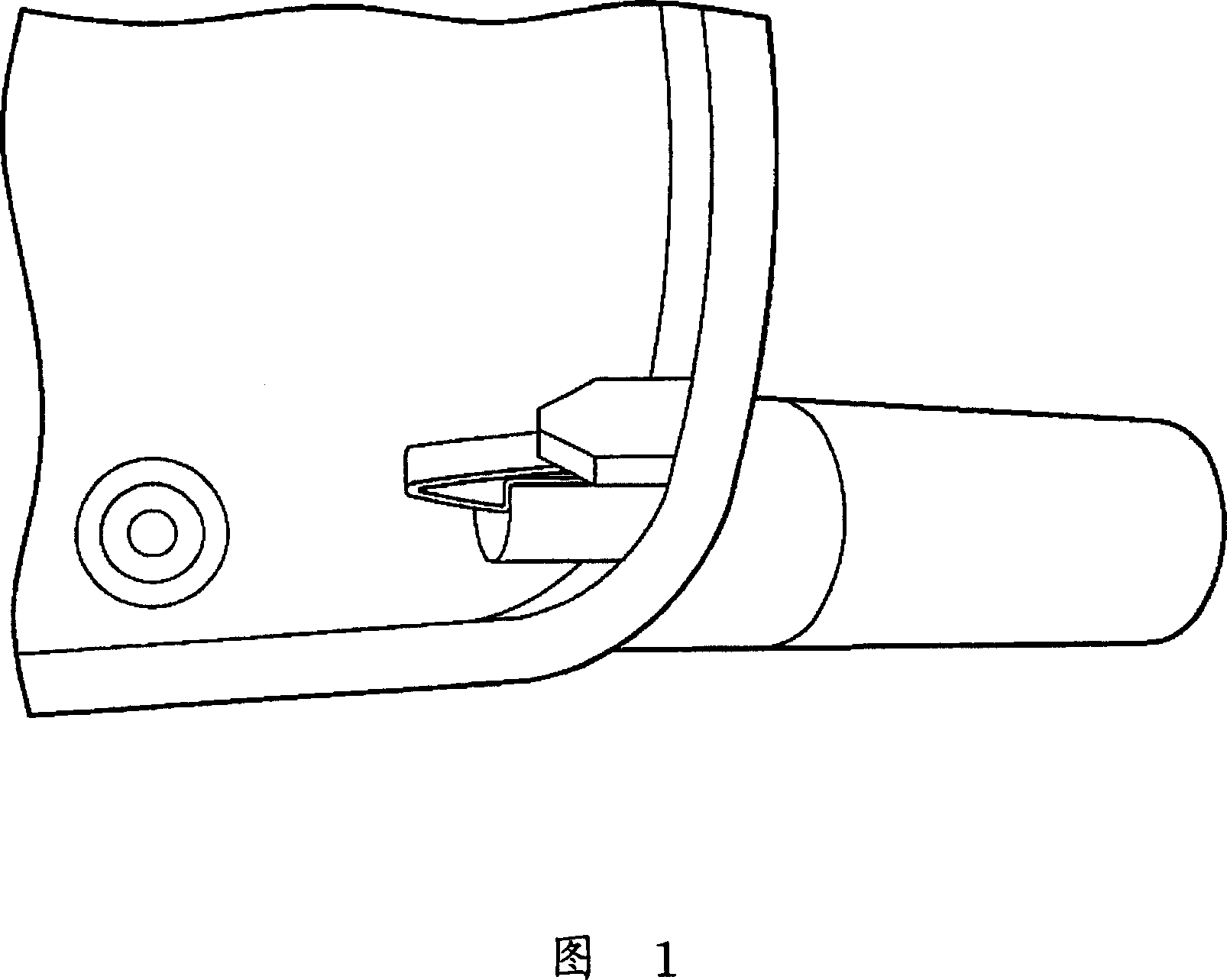
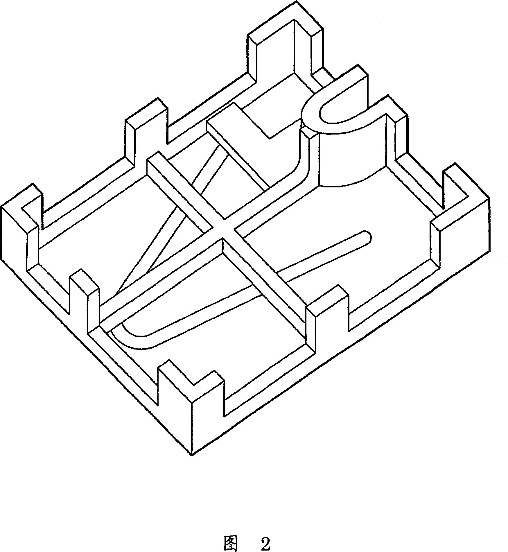
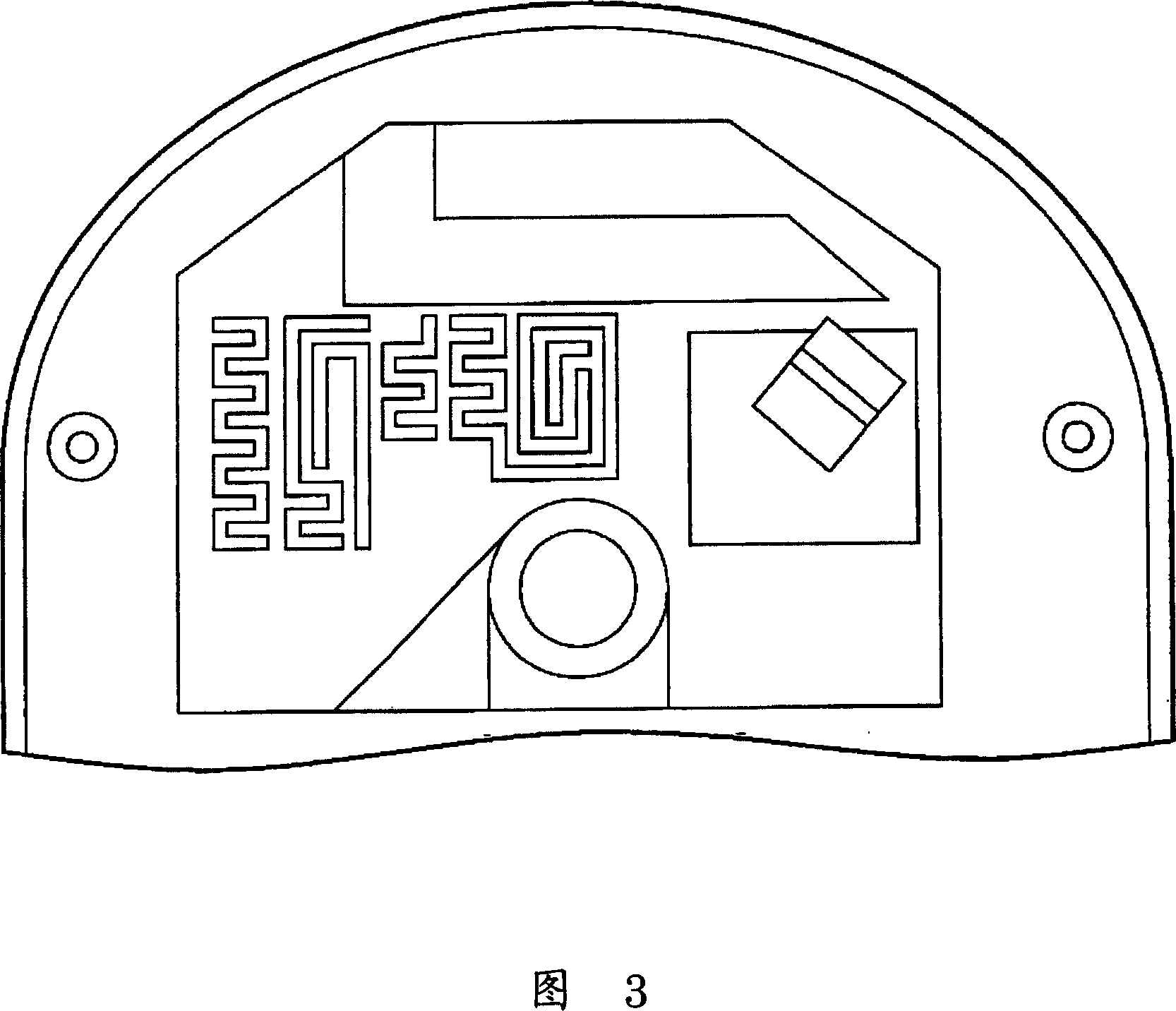
[0029] The antenna structure of the present invention is formed on the shell of the electronic device body, which is different from the method of disposing the antenna inside the body in the prior art.

[0030] In the antenna structure of the present invention, a patterned conductive layer is fabricated on a thin film by using a partial conduction and insulation processing method as an antenna layer for transmitting or receiving wireless signals. The processing method can be: selective electroplating, physical coating, physical coating combined with laser engraving, graphite or carbon powder printing, hot-pressed conductive metal diaphragm, attached conductive metal diaphragm, etc., all kinds of fil...


PUM


Abstract

The invention provides an electron device and antenna structure, said antenna structure includes a film layer, an antenna emitting layer and a backing. The antenna emitting layer is formed on the film layer, the antenna emitting layer and the film layer are combined on the backing, and the antenna emitting layer is between the backing and the film layer. Said backing can be the shell of an electron device, and the antenna emitting layer can be combined on the shell of the electron device in emitting in mould mode. The electron device and antenna structure in the invention can decrease the cost of mould and material of metal piece, but also increase the quality ratio and consistency.

Description

technical field [0001] The present invention relates to an antenna structure, and more particularly to an antenna structure formed on a casing of an electronic device. Background technique [0002] The antenna is a part that performs electromagnetic conversion on radio transmitting and receiving equipment. On handheld electronic products, antennas can be roughly divided into two categories: exposed and hidden. As shown in Figure 1, the exposed antenna protrudes from the body of the electronic device, while the current common hidden antenna mechanism is designed with iron sheets stamped and installed in the body (as shown in Figure 2), and the antenna layer is formed on the flexible circuit on the board (as shown in FIG. 3 ) and by bending the metal wire to form an antenna emitter installed in the body of the electronic device (as shown in FIG. 4 ). Generally speaking, various known design methods are to manufacture the antenna as an independent part, process it through met...

Claims


Application Information

Patent Timeline
IPC IPC(8): H01Q1/22H01Q1/38
Inventor 侯凯中
Owner LITE ON TECH CORP
Why Eureka
Try Eureka