Apparatus and method for inspecting edge defect and discoloration of glass substrate

A glass substrate, edge defect technology, applied in the field of edge defect and discoloration devices, capable of solving problems such as separation, variation of determination results, inability to perform accurate inspection, etc.

Active Publication Date: 2007-11-07
SEMISYSCO CO LTD
View PDF0 Cites 23 Cited by
  • Summary
  • Abstract
  • Description
  • Claims
  • Application Information

AI Technical Summary

Problems solved by technology

[0008] However, conventional glass substrate edge and discoloration inspection devices are separated from TFT-LCD manufacturing devices
Therefore, whenever various processes are performed to manufacture thin film transistor liquid crystal displays, the edge and discoloration inspection of the glass substrate should be repeated and performed individually at a separate site, so it is inconvenient and takes unnecessary time
[0009] In addition, since the discoloration inspection device irradiates light of a specific wavelength to the glass substrate to visually confirm the fringes expressed by the surface of the glass substrate and the reflection angle of the incident light, its determination result may vary depending on the subjectivity of the observer, thus Unable to perform exact check

Method used


Image

  • Apparatus and method for inspecting edge defect and discoloration of glass substrate
  • Apparatus and method for inspecting edge defect and discoloration of glass substrate
  • Apparatus and method for inspecting edge defect and discoloration of glass substrate

Examples


Embodiment Construction

[0037] Now, embodiments of the present invention will be described in detail, examples of which are shown in the accompanying drawings.

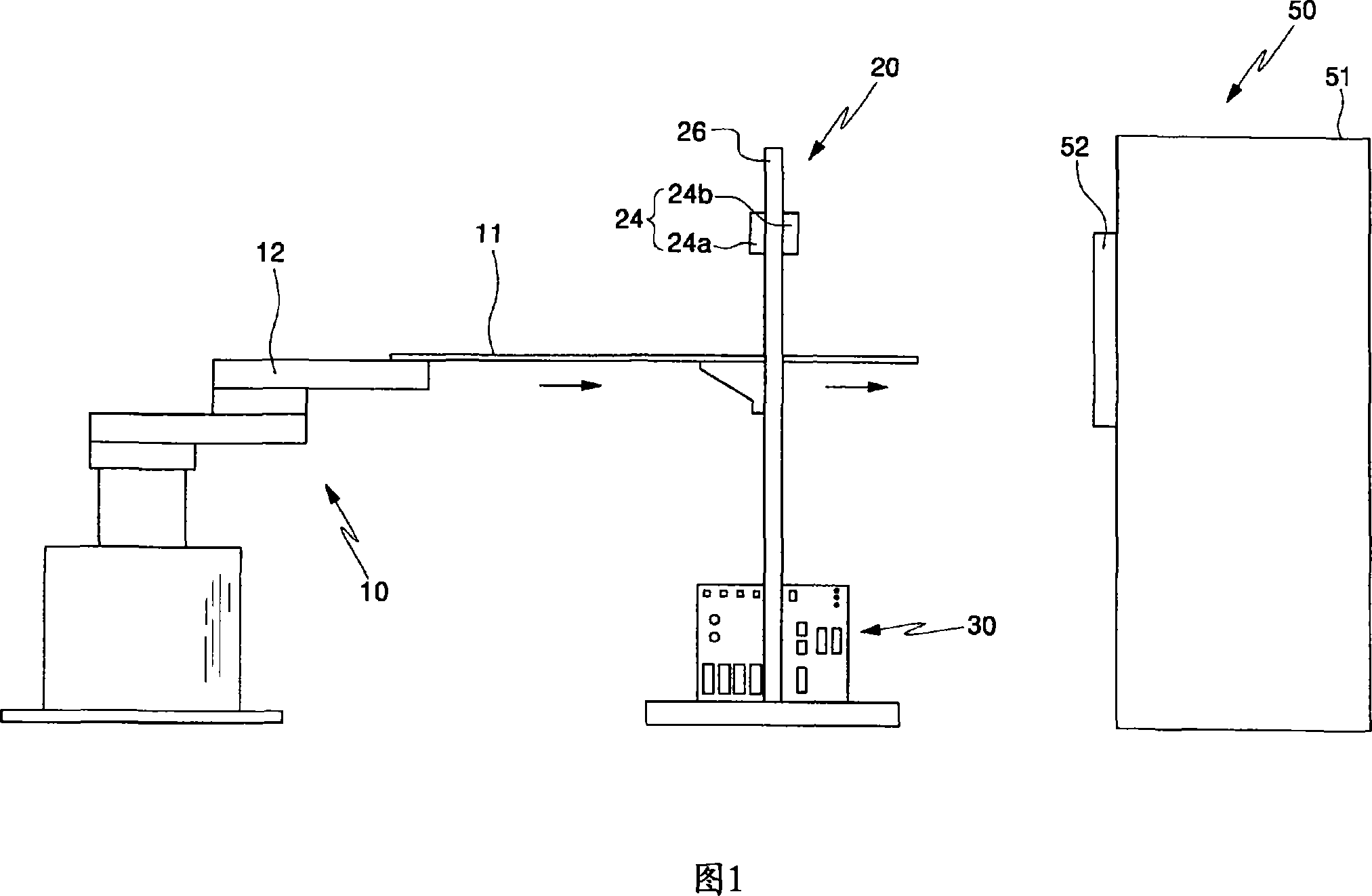
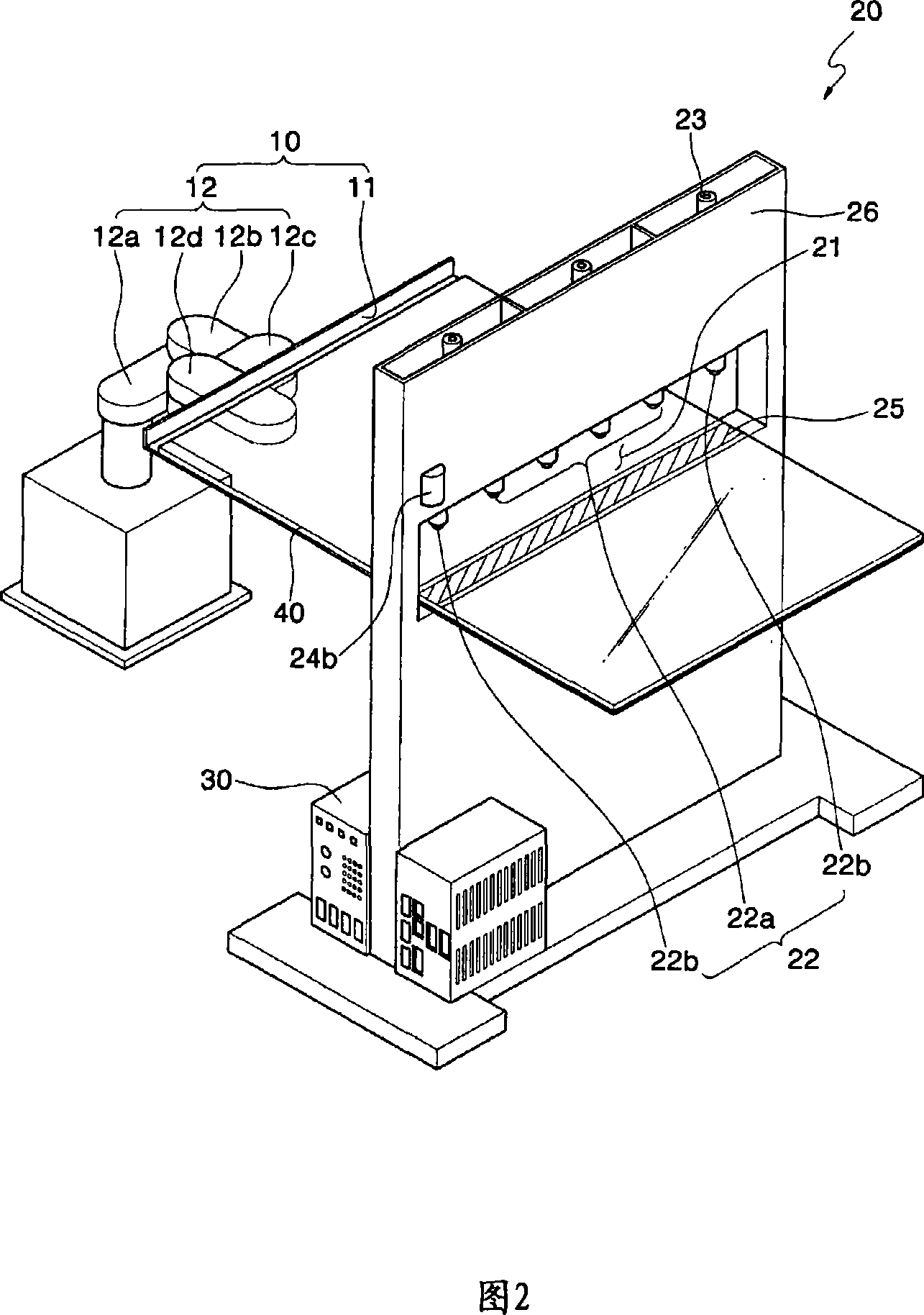
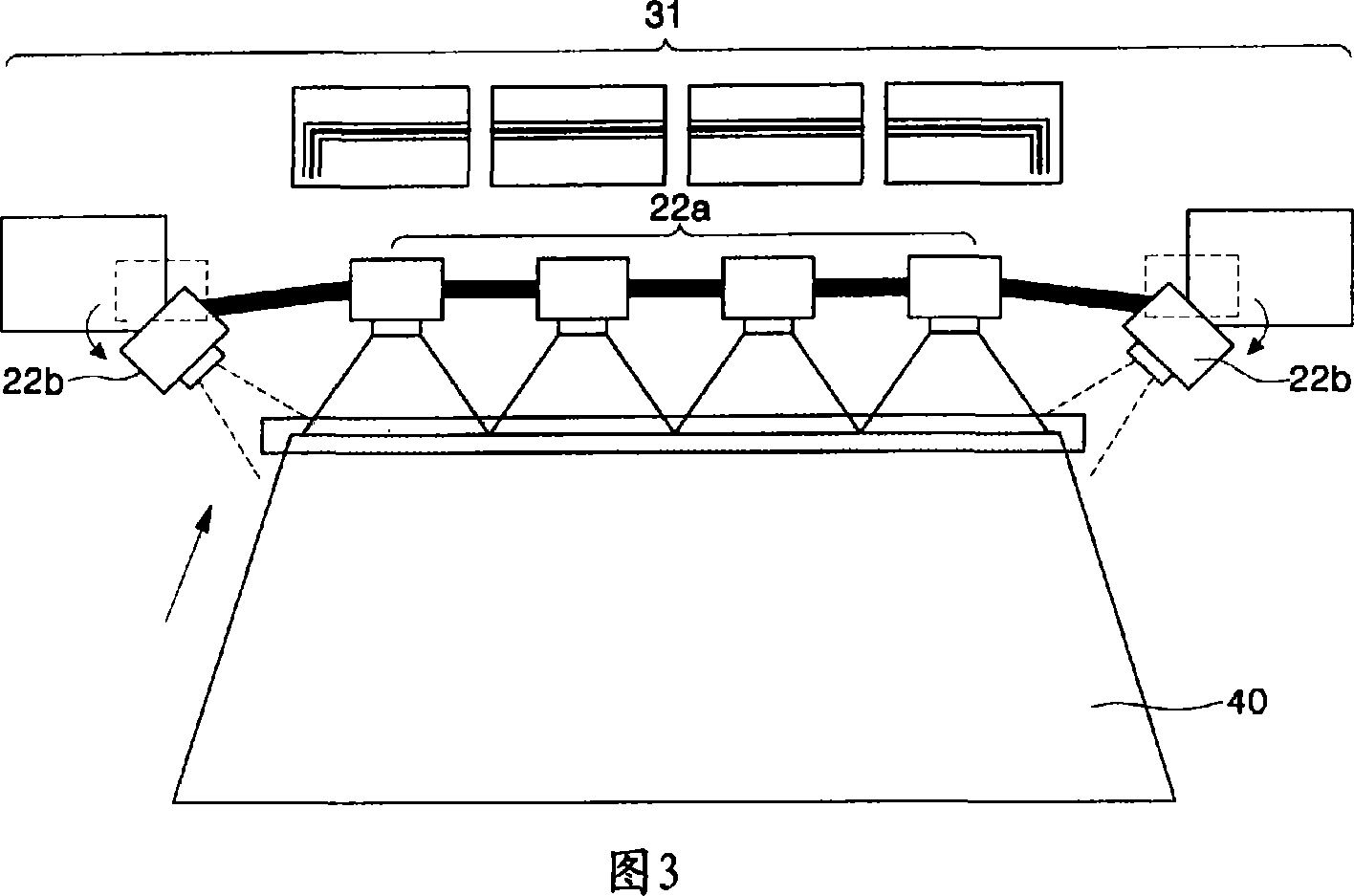
[0038] 1 is a side view of an edge defect and discoloration inspection device according to the present invention, which is installed in front of a gate valve (gate valve) of a deposition or etching device for manufacturing a thin film transistor liquid crystal display, and FIG. Perspective view of the edge defect and discoloration inspection device of the embodiment.

[0039] 1 and 2, the edge defect and discoloration inspection device is selectively installed before the inlet gate valve 52 or after the outlet gate valve (not shown) of the processing equipment 50 using plasma Deposition, etching and sputtering processes are performed to use plasma to manufacture thin film transistor liquid crystal displays.

[0040] The reason for this is to inspect the edge defects and discoloration of the glass substrate 40 before the glass substrate 40 e...


PUM


Abstract

Provided are an apparatus and method for inspecting an edge defect and discoloration. The apparatus includes a loading unit for conveying a glass substrate used to manufacture a thin film transistor liquid crystal display; an inspection unit for inspecting edge defects and discoloration of the glass substrate conveyed by the loading unit; and a control unit for controlling the loading unit and the inspection unit. The edge defect and discoloration inspection apparatus is capable of automatically performing edge defect and discoloration inspection of a glass substrate during processes of manufacturing a thin film transistor liquid crystal display. In addition, it is possible to dispose the edge defect and discoloration inspection apparatus between deposition, etching and sputtering processes to confirm whether the glass substrate is good or bad in real time, thereby performing an economic and rapid process.

Description

technical field [0001] The present invention relates to an apparatus and method for inspecting edge defects and discoloration (discoloration) of a glass substrate, and more particularly, to a method for inspecting thin film transistors and color filters used in thin film transistor liquid crystal displays (TFT-LCDs). Apparatus and methods for edge defects and discoloration of glass substrates for devices. Background technique [0002] Generally, a thin film transistor liquid crystal display is composed of a lower glass substrate, an upper glass substrate, and liquid crystal injected between the lower glass substrate and the upper glass substrate. A thin film transistor is formed on the lower glass substrate, and a color filter is formed on the upper glass substrate. [0003] When defects such as cracks or edge breakages occur in the glass substrates used to construct thin film transistors and color filters, the entire thin film substrate may be broken...

Claims


Application Information

Patent Timeline
Patent Type & Authority Applications(China)
IPC IPC(8): G02F1/13
CPCG01N21/27G01N21/896G02F2001/133302G02F1/1309G01N2021/9513G02F1/133302A47J31/441A47J31/46A47J31/54A47J36/14A47J36/38
Inventor 李淳钟禹奉周
Owner SEMISYSCO CO LTD
Why Eureka
Try Eureka