Method for preparing tin-oxide mono-crystal film
A single crystal thin film and tin oxide technology, applied in the field of preparation of tin oxide single crystal thin films, can solve the problems of difficult to obtain tin oxide thin film materials with inter-band emission properties, difficult to obtain performance P-type tin oxide thin film materials, and many film defects. , to achieve the effects of easy and precise control of process conditions, excellent optoelectronic properties, and easy P-type doping
- Summary
- Abstract
- Description
- Claims
- Application Information
AI Technical Summary
Benefits of technology
Problems solved by technology
Method used
Image
Examples
Embodiment 1
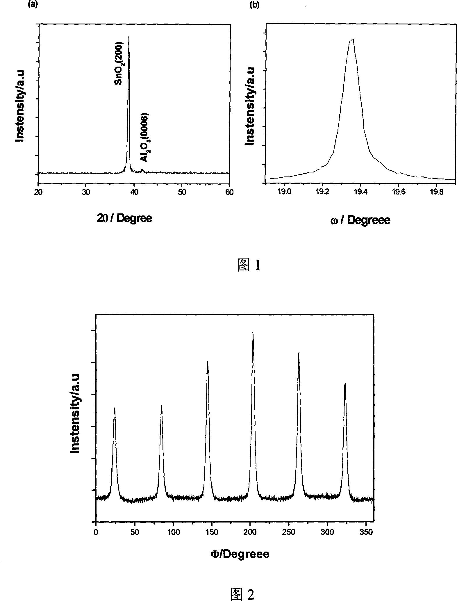
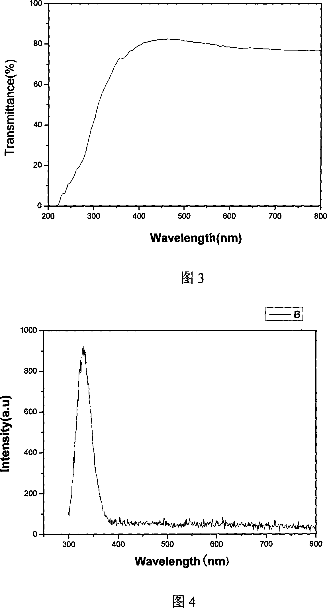
[0044] Example 1: Tin oxide single crystal thin film material was prepared by MOCVD technology.
[0045] (1) First pump the reaction chamber of the MOCVD equipment to a high vacuum state of 5×10 -4 Pa, heat the sapphire substrate to 650°C;
[0046] (2) Open the valve of the nitrogen cylinder and feed nitrogen into the reaction chamber (background N 2 ) 400sccm, 30 minutes, make reaction chamber pressure be 50Torr;
[0047](3) Open the valve of the oxygen cylinder, adjust the flow rate of oxygen to 50 sccm, and keep it for 10 minutes;
[0048] (4) Use tetraethyltin [Sn(C 2 h 5 ) 4 ] As an organometallic source, open the valve of the tin source bottle, adjust the flow rate of carrier gas (nitrogen) to 30 sccm, and keep for 10 minutes;
[0049] (5) Pass oxygen and organometallic tin sources into the reaction chamber simultaneously, and keep the film growth time as 180 minutes;
[0050] (6) Close the valves of the tin source bottle and the oxygen bottle after the reaction, ...
Embodiment 2
[0053] Embodiment 2: comparative example
[0054] MOCVD technology prepares tin oxide thin film material, and preparation method and processing condition are identical with embodiment 1, just be substrate material with the single crystal silicon chip of polishing, use Sn(C 2 h 5 ) 4 As an organometallic source, the tin oxide film prepared under the condition of 650°C has a polycrystalline structure, the film growth time is 180 minutes, and the film thickness is 120nm. The carrier mobility is 11cm 2 V -1 S -1 , the average relative transmittance in the visible light range exceeds 83%. No luminescence generated by interband transitions was observed in room temperature photoluminescence spectroscopy.
Embodiment 3
[0055] Embodiment 3: comparative example
[0056] MOCVD technology prepares tin oxide thin film material, and preparation process condition is identical with embodiment 1, and difference is that the single crystal quartz of polishing is substrate material, uses Sn(C 2 h 5 ) 4 As an organometallic source, the tin oxide film prepared at 650°C has a polycrystalline structure, the film growth time is 180 minutes, and the film thickness is 115nm. The thin film carrier mobility is 8cm 2 V -1 S -1 , the average relative transmittance in the visible light range exceeds 83%. No luminescence generated by interband transitions was observed in room temperature photoluminescence spectroscopy.
PUM
| Property | Measurement | Unit |
|---|---|---|
| Thickness | aaaaa | aaaaa |
| Carrier mobility | aaaaa | aaaaa |
| Carrier mobility | aaaaa | aaaaa |
Abstract
Description
Claims
Application Information
 - R&D
- Intellectual Property
- Life Sciences
- Materials
- Tech Scout
- Unparalleled Data Quality
- Higher Quality Content
- 60% Fewer Hallucinations
Browse by: Latest US Patents, China's latest patents, Technical Efficacy Thesaurus, Application Domain, Technology Topic, Popular Technical Reports.
© 2025 PatSnap. All rights reserved.Legal|Privacy policy|Modern Slavery Act Transparency Statement|Sitemap|About US| Contact US: help@patsnap.com


