Eureka AIR delivers breakthrough ideas for toughest innovation challenges, trusted by R&D personnel around the world.

Semiconductor device and its forming method

一种半导体、器件的技术,应用在双极器件结构领域,能够解决双极器件最大振荡频率限制等问题,达到降低寄生电阻、消除电阻负荷、降低结温度的效果

Active Publication Date: 2007-11-28
INT BUSINESS MASCH CORP
View PDF1 Cites 12 Cited by
  • Summary
  • Abstract
  • Description
  • Claims
  • Application Information

AI Technical Summary

Problems solved by technology

The total parasitic resistance of conventional bipolar devices is significant because of the relatively high resistance of the semiconductor material forming the above-mentioned conductive paths in conventional bipolar devices, thus increasing with the device cut-off frequency (f t ) increases, the maximum oscillation frequency of the bipolar device (f max ) to limit

Method used


Image

  • Semiconductor device and its forming method
  • Semiconductor device and its forming method
  • Semiconductor device and its forming method

Examples


Embodiment Construction

[0036] In the following description, numerous specific details are set forth, such as particular structure, components, materials, dimensions, process steps and techniques, in order to provide the reader with a thorough understanding of the present invention. However, it will be appreciated by those skilled in the art that the present invention may be practiced without these specific details. In other instances, well-known structures or process steps have not been described in detail in order not to obscure the invention.

[0037] It will be understood that when an element such as a layer, region or substrate is referred to as being "on" or "over" another element, it can be directly on the other element or intervening elements may also be present. In contrast, when an element is referred to as being "directly on" or over another element, there are no intervening elements present. It will also be understood that when an element is referred to as being "under" or "under" anothe...


PUM


Abstract

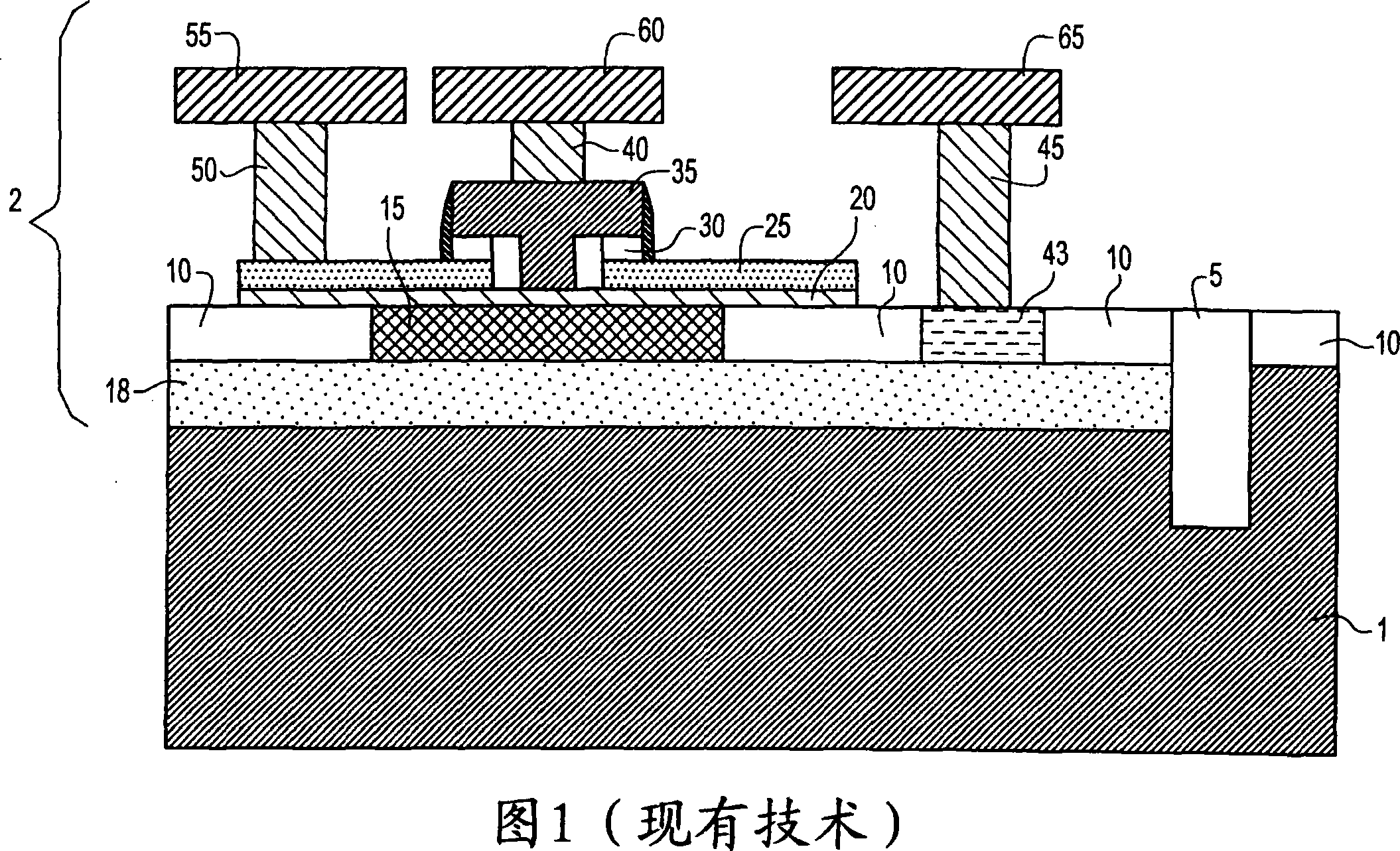
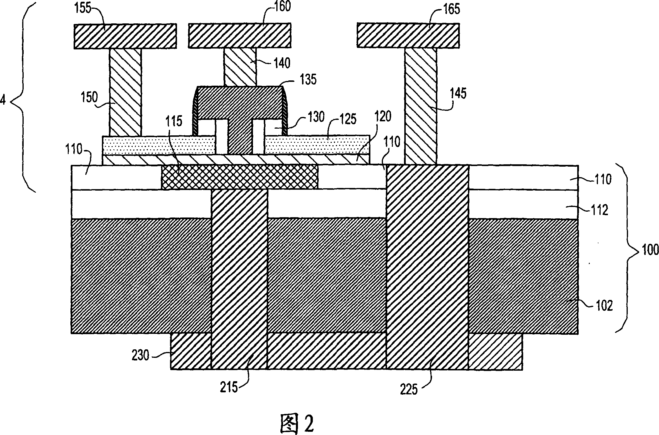
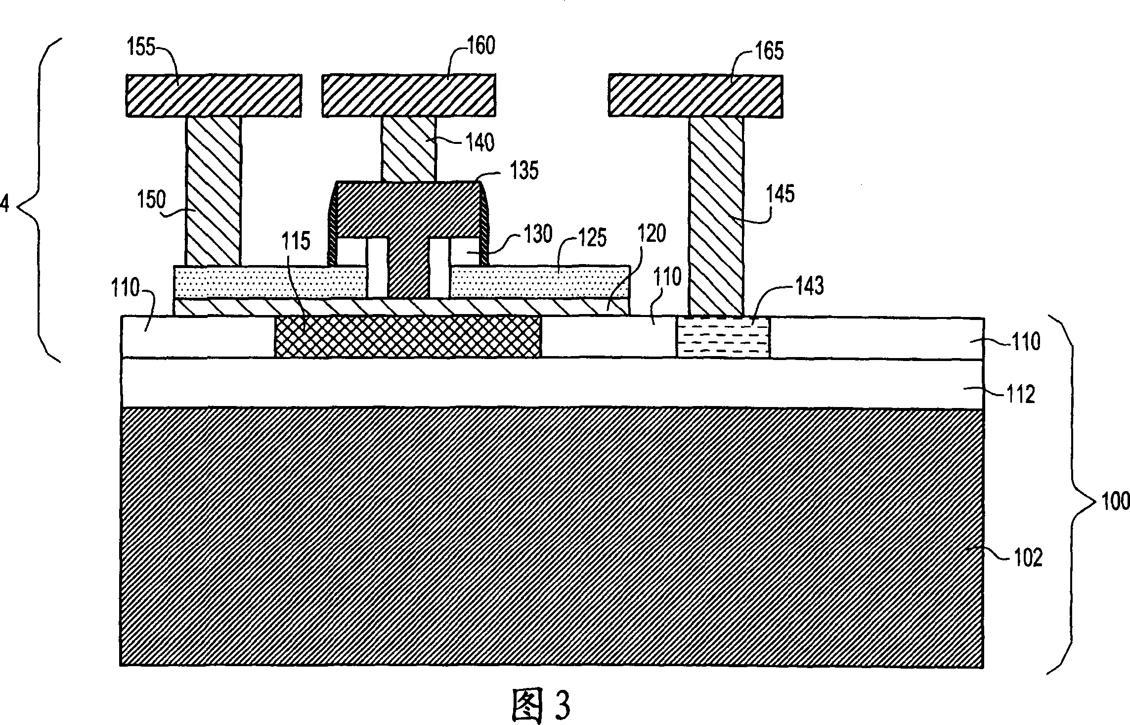
The present invention relates to a device structure that comprises a substrate with front and back surfaces, and at least one semiconductor device with a first conductive structure located in the substrate and a second conductive structure located thereover. A first conductive contact is located over the front surface of the substrate and laterally offset from the first conductive structure. The first conductive contact is electrically connected to the first conductive structure by a conductive path that extends: (1) from the first conductive structure through the substrate to the back surface, (2) across the back surface, and (3) from the back surface through the substrate to the first conductive contact on the front surface. Further, a second conductive contact is located over the front surface and is electrically connected to the second conductive structure. The conductive path can be formed by lithography and etching followed by metal deposition.

Description

technical field [0001] The present invention generally relates to semiconductor device structures. More particularly, the present invention relates to bipolar device structures having back contacts for improved heat dissipation and reduced parasitic resistance. Background technique [0002] Bipolar junction transistors (BJTs) and varactors (varactors) are playing an increasingly important role in the semiconductor industry. Bipolar circuit performance, especially the improvement of operating speed is the basic requirement to improve the network communication system and wireless system. BJTs with silicon-germanium bases provide ideal device performance for such systems. For example, a current cut-off frequency (f t ). [0003] As the current density in bipolar circuits increases, the heat dissipation and parasitic resistance of bipolar devices create more significant limitations on device performance. High junction temperature and collector resistance make f t decreases...

Claims


Application Information

Patent Timeline
Patent Type & Authority Applications(China)
IPC IPC(8): H01L29/73H01L29/737H01L29/417H01L23/367H01L21/331H01L21/28
CPCH01L23/481H01L29/41708H01L29/7371H01L2924/12044H01L2924/0002H01L21/76898H01L2924/00
Inventor 库纳尔·威地吕在成理查德·P.·沃朗特弗朗索瓦·帕日蒂
Owner INT BUSINESS MASCH CORP
Why Eureka
Eureka Blog
Learn More