Process and fabrication methods for emitter wrap through back contact solar cells

A solar cell, back contact technology, applied in semiconductor/solid-state device manufacturing, circuits, electrical components, etc., can solve problems such as etching, laser damage, etc., and achieve the effect of economical process steps

Inactive Publication Date: 2007-12-12
ADVENT SOLAR INC
View PDF8 Cites 20 Cited by
  • Summary
  • Abstract
  • Description
  • Claims
  • Application Information

AI Technical Summary

Problems solved by technology

[0015] 6. Laser damage etching and cleaning
Technical issues include patterning of doped layers (if present), surface passivation between negative and positive contact areas, and application of negative and positive polarity contacts

Method used


Image

  • Process and fabrication methods for emitter wrap through back contact solar cells
  • Process and fabrication methods for emitter wrap through back contact solar cells
  • Process and fabrication methods for emitter wrap through back contact solar cells

Examples


Embodiment Construction

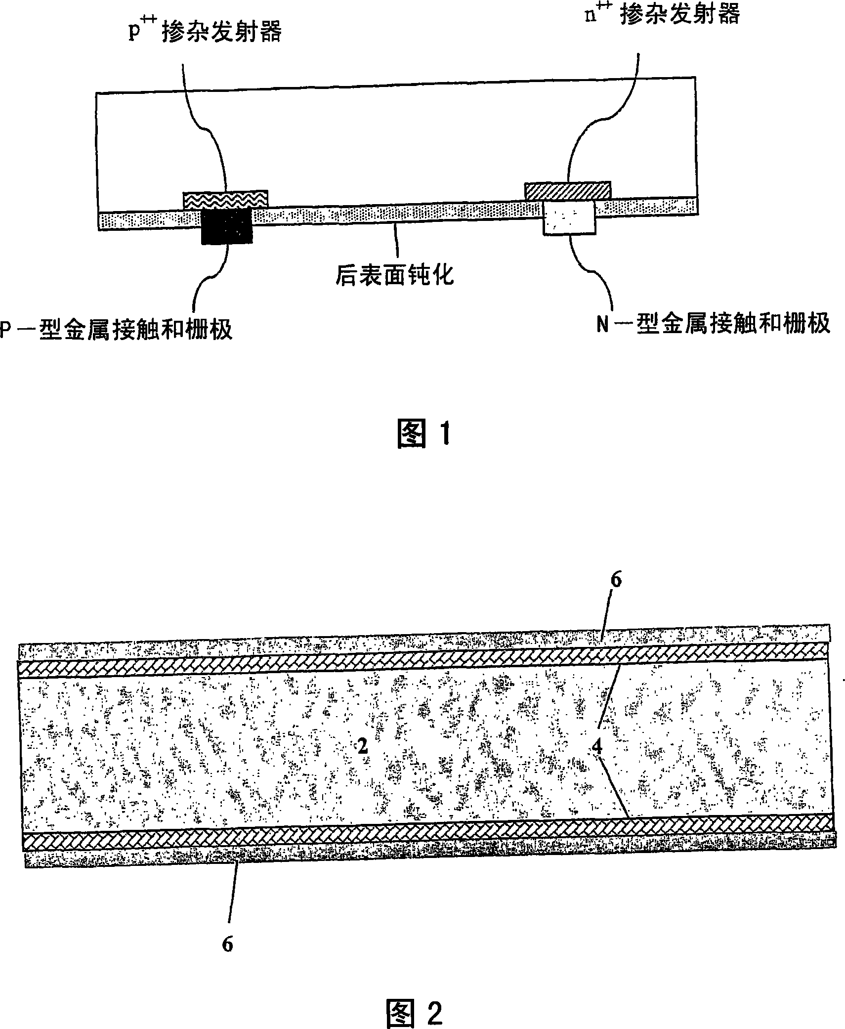
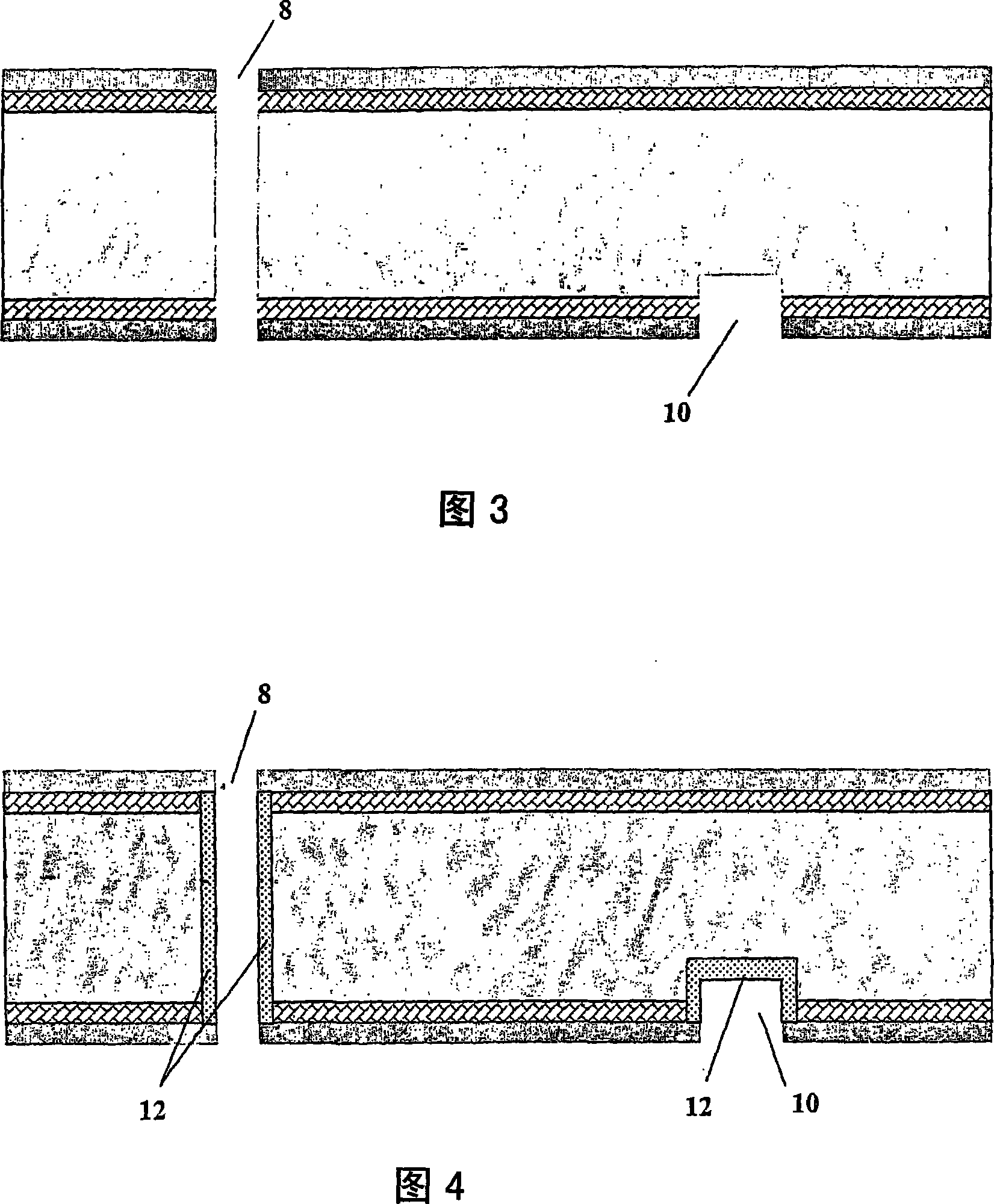
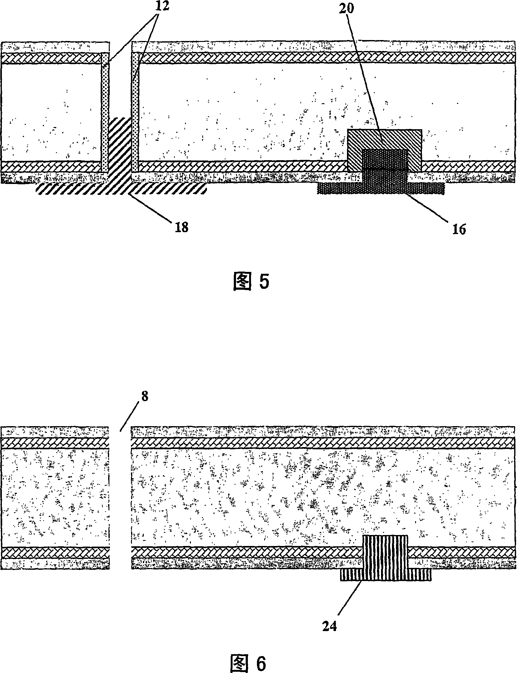
[0046] The invention disclosed herein provides improved processes and methods for fabricating back contact solar cells, and in particular provides methods and processes for more economical manufacture. It should be understood that although a number of different discrete methods are disclosed, one skilled in the art can combine or alter two or more methods, thereby providing an alternative method of preparation. It should also be understood that while the figures and example process steps describe the fabrication of back contact emitter wrap-through cells, these process steps can be used to fabricate other back contact solar cell structures such as MWT, MWA or back junction solar cells.

[0047] The process of the present invention preferably uses a laser to pattern the p-type contacts (laser scribing) rather than patterning a printed (ie screen printed) diffusion barrier material applied in a suitable pattern. Patterned screen-printed diffusion barriers provide low-quality int...


PUM


Abstract

Back contact solar cells including rear surface structures and methods for making same. The rear surface is doped to form an n<+> emitter and then coated with a dielectric layer. Small regions are scribed in the rear surface and p-type contacts are then formed in the regions. Large conductive grid areas overlay the dielectric layer. The methods provide for increasing efficiency by minimizing p-type contact areas and maximizing n-type doped regions on the rear surface of a p-type substrate.

Description

[0001] Cross References to Related Applications [0002] This application claims priority to and the benefit of the following patent applications: U.S. Provisional Patent Application Serial No. 60 / 607,984, filed September 7, 2004, entitled "Improved Process and Method of Making Emitter Wrapped Back Contact Solar Cells" ” and U.S. Provisional Patent Application Serial No. 60 / 707,648, filed August 11, 2005, entitled “Further Improved Process and Fabrication of Emitter Wrap-Through Back-Contact Solar Cells.” This application is also a continuation-in-part of the following U.S. patent applications, both filed February 3, 2005: Ser. Embedded Contact Solar Cells with Heterogeneous Contacts," and Serial No. 11 / 050,184, entitled "Contact Fabrication of Emitter Wrapped Back-Contacted Silicon Solar Cells," these applications claim the benefit of the following patent application docket: filed on February 5, 2004 U.S. Provisional Patent Application Serial No. 60 / 542,390, entitled "Fabricat...

Claims


Application Information

Patent Timeline
Patent Type & Authority Applications(China)
IPC IPC(8): H01L21/8242
Inventor 彼得・哈克詹姆斯・M・吉
Owner ADVENT SOLAR INC
Why Eureka
Try Eureka