Chip detection method

A detection method and wafer technology, which are applied in the direction of measuring electricity, measuring devices, measuring electrical variables, etc., can solve the problems of reduced production efficiency, false alarms, and increased production costs, so as to reduce the number of false alarms, reduce production costs, and improve production. The effect of efficiency

Inactive Publication Date: 2007-12-19
SEMICON MFG INT (SHANGHAI) CORP +1
View PDF1 Cites 43 Cited by
  • Summary
  • Abstract
  • Description
  • Claims
  • Application Information

AI Technical Summary

Problems solved by technology

[0013] The actual production found that due to factors such as the design and layout of the semiconductor device, there are differences in the properties allowed by the process between the central area of ​​the wafer and the edge area. After image processing, it shows that the gray value of the central area and the edge area has a significant difference; and the whole wafer has only one standard chip, and it is generated based on the gray levels of all the chips of the whole wafer, then it will inevitably cause edge or The gray value of the color in the central area is quite different from the gray value of the standard chip. The color difference caused by normal factors is mistaken for the color difference caused by defects. The existence of this phenomenon can easily cause false alarms during the detection process. , the original normal chip is judged as a defective chip, resulting in a decrease in production efficiency and an increase in production cost

Method used


Image

  • Chip detection method
  • Chip detection method
  • Chip detection method

Examples


Embodiment Construction

[0047] In order to make the above objects, features and advantages of the present invention more comprehensible, specific implementations of the present invention will be described in detail below in conjunction with the accompanying drawings.

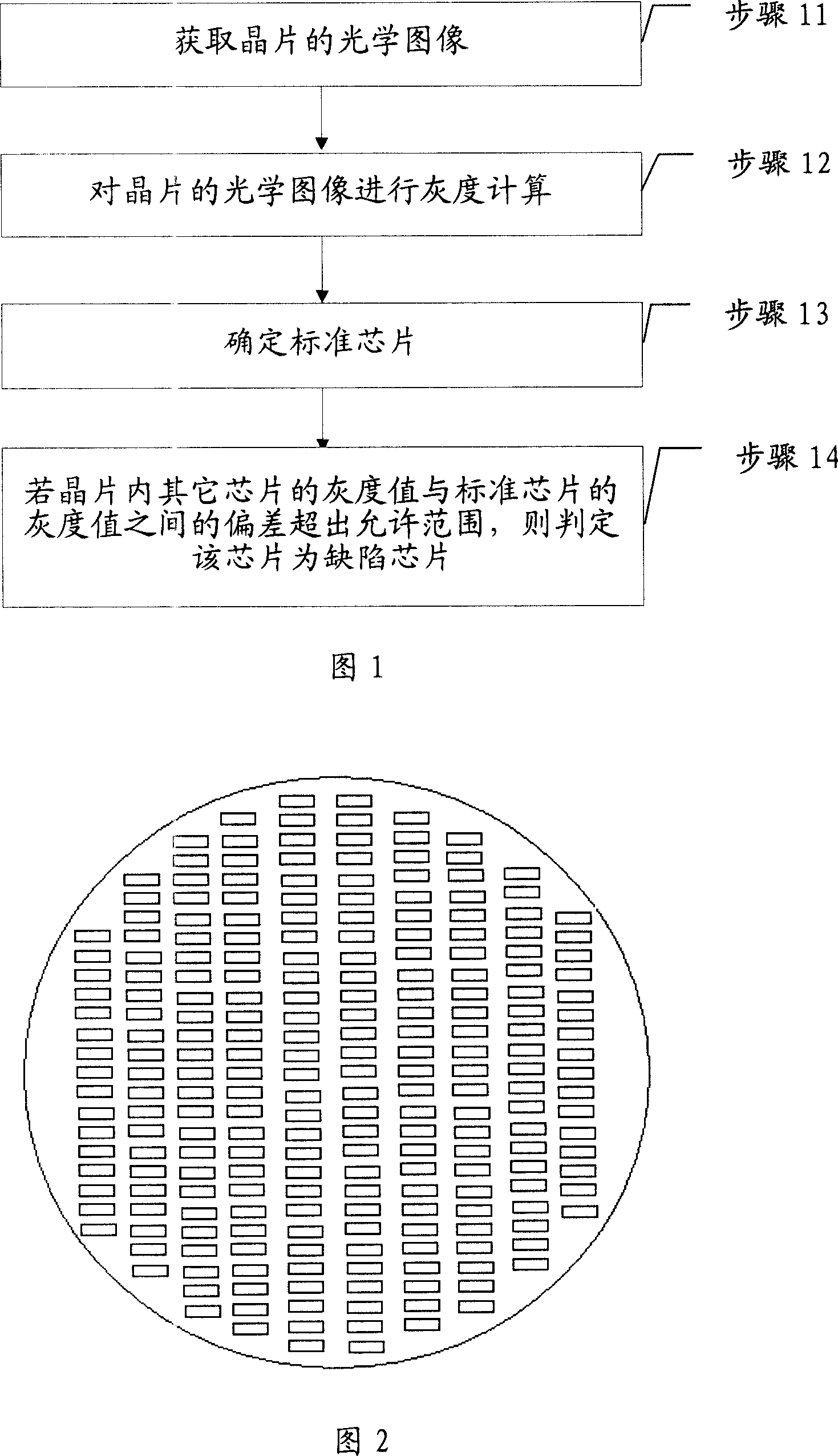
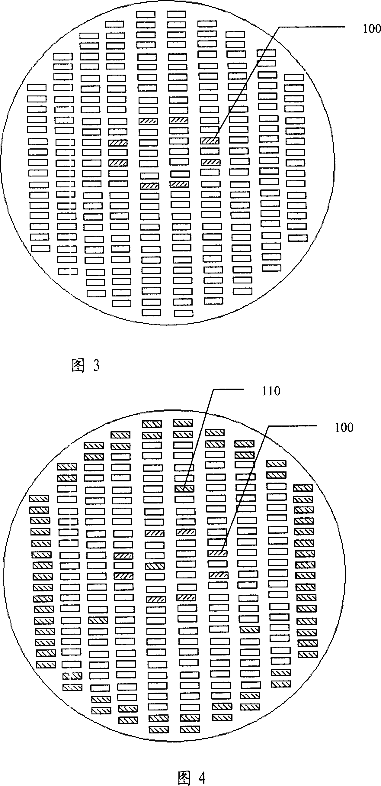
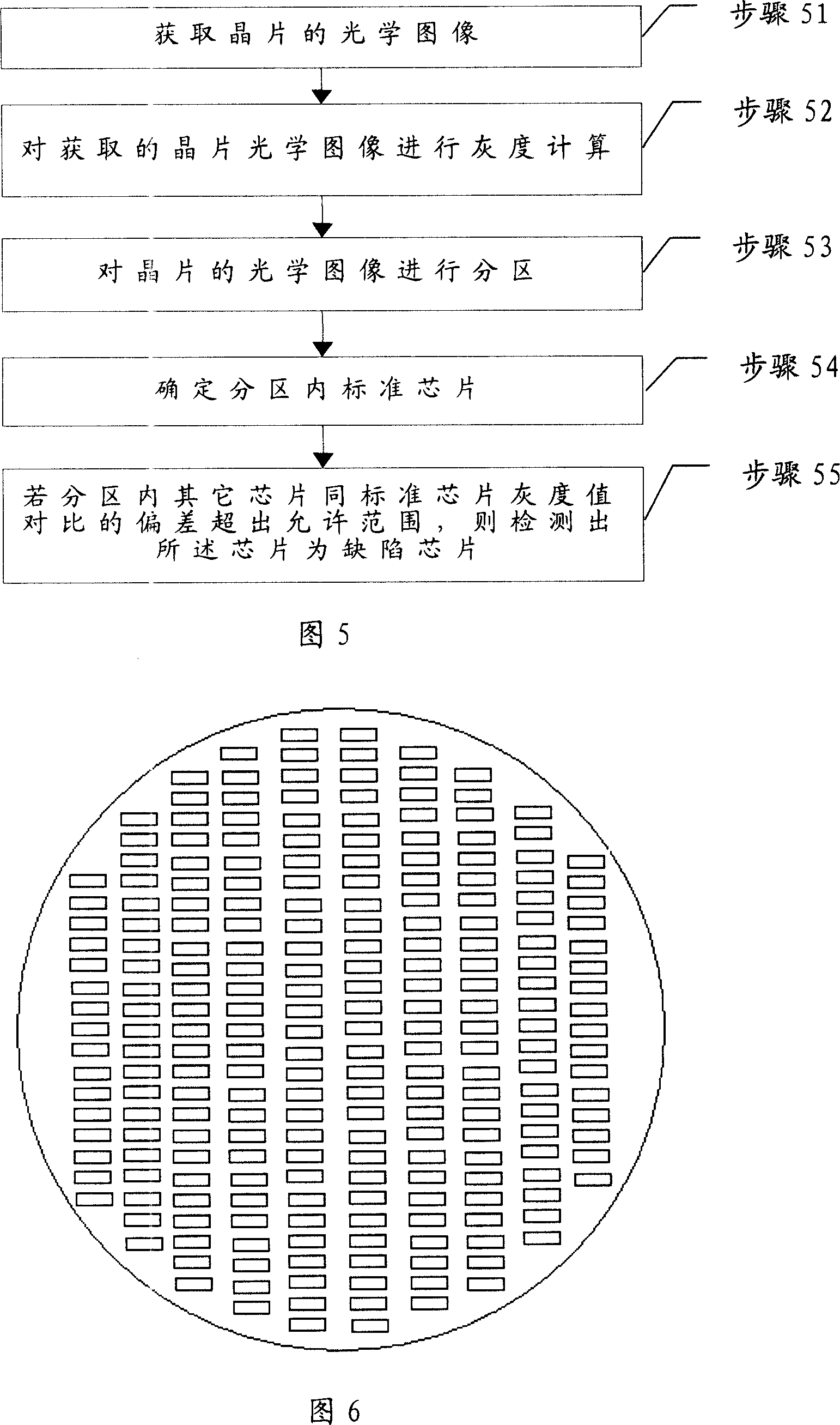
[0048] The wafer inspection method provided by the present invention includes: acquiring an optical image of the wafer; performing grayscale calculation on the optical image of the wafer and performing partitioning; determining the standard chip in the partition; comparing the grayscale values ​​of other chips in the partition with the standard chip , if the comparison result exceeds the allowable range, it is detected that the chip is a defective chip.

[0049] Fig. 5 is a schematic diagram illustrating the automatic visual inspection process of the embodiment of the present invention. As shown in Fig. 5, the automatic visual inspection process of the first embodiment of the present invention is:

[0050] Step 51: Using the optical pr...


PUM


Abstract

This invention discloses a test method for wafers including: utilizing an optical process unit in an AVI tool to get an optical image of a wafer, carrying out grey computation to the image and dividing it to several zones, selecting a subarea standard chip, finally, carrying out contrast of grey values to other chips in different areas with the standard one to test defect chips, in which, the mode of partition is decided according to the state of products, a subarea can be any area in the image and the standard chip may be one existing in the chip or a virtual chip model got by the AVI tool, and a judgment standard should be designed in advance before contrasting grey values.

Description

technical field [0001] The invention relates to the technical field of semiconductor manufacturing, in particular to a wafer detection method. Background technique [0002] In the semiconductor manufacturing process, wafer defects are mainly determined through optical inspection technology, and the cause of defects is further tracked, thereby improving the production process and increasing product yield. Obviously, wafer inspection is an important step in the actual production process. The Chinese patent application with the application number "98115227.9" mentioned that in the semiconductor manufacturing process, automatic methods are often used to detect wafer defects. [0003] Fig. 1 is a schematic diagram of an automatic visual inspection process in the prior art. As shown in Fig. 1, the specific steps of the automatic visual inspection in the prior art include: [0004] Step 11: Obtain an optical image of the wafer using the optical processing unit in the AVI tool. I...

Claims


Application Information

Patent Timeline
Patent Type & Authority Applications(China)
IPC IPC(8): H01L21/66G01N21/95G01R31/00
Inventor 左仲王明珠吕秋玲赵庆国
Owner SEMICON MFG INT (SHANGHAI) CORP
Why Eureka
Try Eureka